AD549
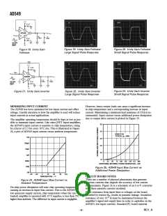
Figure 19. Unity Gain Follower
Large Signal Pulse Response
Figure 20. Unity Gain Follower
Small Signal Pulse Response
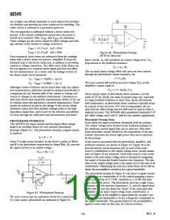
Figure 18. Unity Gain
Follower
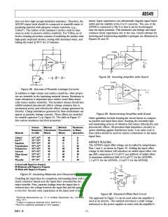
Figure 23. Unity Gain Inverter
Small Signal Pulse Response
Figure 22. Unity Gain Inverter
Large Signal Pulse Response
Figure 21. Unity Gain Inverter
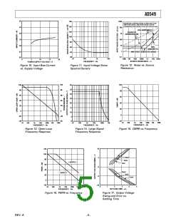
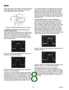
MINIMIZING INPUT CURRENT
However, heavy output loads can cause a significant increase
in chip temperature and a corresponding increase in input
current. Maintaining a minimum load resistance of 10 Ω is rec-
ommended. Input current versus additional power dissipation
due to output drive current is plotted in Figure 25.
The AD549 has been optimized for low input current and offset
voltage. Careful attention to how the amplifier is used will reduce
input currents in actual applications.
The amplifier operating temperature should be kept as low as pos-
sible to minimize input current. Like other JFET input amplifiers,
the AD549’s input current is sensitive to chip temperature, rising
by a factor of 2.3 for every 10°C rise. This is illustrated in Figure
24, a plot of AD549 input current versus ambient temperature.
6.0
5.0
BASED ON
TYPICAL I = 40fA
B
1nA
100pA
10pA
1pA
4.0
3.0
2.0
1.0
100fA
10fA
1fA
0
25
50
75 100 125 150 175 200
ADDITIONAL INTERNAL POWER DISSIPATION – mW
Figure 25. AD549 Input Bias Current vs.
Additional Power Dissipation
–55
–25
5
35
65
95
125
TEMPERATURE – °C
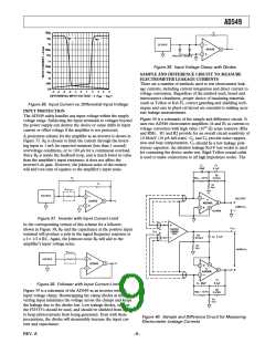
CIRCUIT BOARD NOTES
There are a number of physical phenomena that generate
spurious currents that degrade the accuracy of low current
measurements. Figure 26 is a schematic of an I-to-V converter
with these parasitic currents modeled.
Figure 24. AD549 Input Bias Current vs.
Ambient Temperature
On-chip power dissipation will raise chip operating temperature
causing an increase in input bias current. Due to the AD549’s
low quiescent supply current, chip temperature when the (un-
loaded) amplifier is operated with 15 V supplies, is less than 3°C
higher than ambient. The difference in input current is negligible.
Finite resistance from input lines to voltages on the board,
modeled by resistor RP, results in parasitic leakage. Insulation
resistance of over 1015 Ω must be maintained between the
amplifier’s signal and supply lines in order to capitalize on the
AD549’s low input currents. Standard PC board material
–6–
REV. A

 ADI [ ADI ]