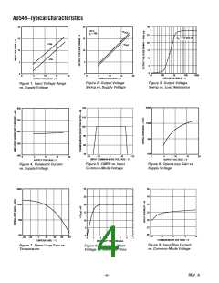
AD549
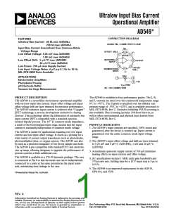
Model
AD549J
Typ
AD549K
Typ
AD549L
Typ
AD549S
Typ
Min
Max
Min
Max
Min
Max
Min
Max
Units
POWER SUPPLY
Rated Performance
Operating
±15
±15
±15
±15
V
V
؎5
؎18
؎5
؎18
؎5
؎18
؎5
؎18
Quiescent Current
0.60
0.70
0.60
0.70
0.60
0.70
0.60
0.70
mA
TEMPERATURE RANGE
Operating, Rated Performance
Storage
0
–65
+70
+150
0
–65
+70
+150
0
–65
+70
+150
–55
–65
+125
+150
°C
°C
PACKAGE OPTION
TO-99 (H-08A)
Chips
AD549JH
AD549JChips
AD549KH
AD549LH
AD549SH, AD549SH/883B
NOTES
1Bias current specifications are guaranteed after 5 minutes of operation at TA = +25°C. Bias current increases by a factor of 2.3 for every 10°C rise in temperature.
2Input offset voltage specifications are guaranteed after 5 minutes of operation at TA = +25°C.
3Defined as max continuous voltage between the inputs such that neither input exceeds ±10 V from ground.
Specifications subject to change without notice.
All min and max specifications are guaranteed. Specifications in boldface are tested on all production units at final electrical test. Results from those tests are used to
calculate outgoing quality levels.
ABSOLUTE MAXIMUM RATINGS1
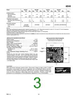
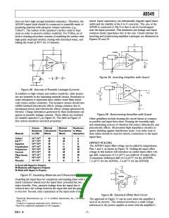
METALIZATION PHOTOGRAPH
Dimensions shown in inches and (mm).
Contact factory for latest dimensions.
Supply Voltage . . . . . . . . . . . . . . . . . . . . . . . . . . . . . . . . ±18 V
Internal Power Dissipation . . . . . . . . . . . . . . . . . . . . . .500 mW
Input Voltage . . . . . . . . . . . . . . . . . . . . . . . . . . . . . . . . . ±18 V2
Output Short Circuit Duration . . . . . . . . . . . . . . . . . Indefinite
Differential Input Voltage . . . . . . . . . . . . . . . . . . +VS and –VS
Storage Temperature Range (H) . . . . . . . . . .–65°C to +125°C
Operating Temperature Range
AD549J (K, L) . . . . . . . . . . . . . . . . . . . . . . . . 0°C to +70°C
AD549S . . . . . . . . . . . . . . . . . . . . . . . . . . –55°C to +125°C
Lead Temperature Range (Soldering 60 sec) . . . . . . . . +300°C
NOTES
1Stresses above those listed under “Absolute Maximum Ratings” may cause
permanent damage to the device. This is a stress rating only and functional
operation of the device at these or any other conditions above those indicated in the
operational section of this specification is not implied. Exposure to absolute
maximum rating conditions for extended periods may affect device reliability.
2For supply voltages less than ±18 V, the absolute maximum input voltage is equal
to the supply voltage.
CAUTION
ESD (electrostatic discharge) sensitive device. Electrostatic charges as high as 4000 V readily
accumulate on the human body and test equipment and can discharge without detection.
Although the AD549 features proprietary ESD protection circuitry, permanent damage may
occur on devices subjected to high energy electrostatic discharges. Therefore, proper ESD
precautions are recommended to avoid performance degradation or loss of functionality.
WARNING!
ESD SENSITIVE DEVICE
REV. A
–3–

 ADI [ ADI ]