BRIGHT
Microelectronics
Inc.
Preliminary BM29F040
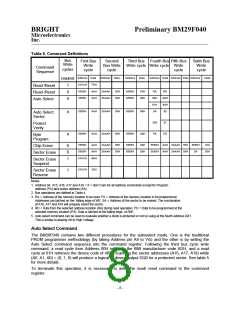
Table 7 Sector Address Table
Sector
SA0
SA1
SA2
SA3
SA4
SA5
SA6
SA7
A18
0
A17
0
A16
0
Address Range
00000H - 0FFFFH
10000H - 1FFFFH
20000H - 2FFFFH
30000H - 3FFFFH
40000H - 4FFFFH
50000H - 5FFFFH
60000H - 6FFFFH
70000H - 7FFFFH
0
0
1
0
1
0
0
1
1
1
0
0
1
0
1
1
1
0
1
1
1
Data Flags
DQ7 Data polling
The BM29F040 features Data polling to indicate to the host system that the Embedded Algorithms are
in progress or completed. During the Embedded Program Algorithm, an attempt to read the device
will produce the complement of the Data last written to DQ7. Upon completion of the Embedded
Programming Algorithm an attempt to read the device will produce the true data last written to DQ7.
Data polling is valid after the rising edge of the fourth WE pulse in the four write pulse sequence.
During the Embedded Erase Algorithm, DQ7 will be "0" until the Erase operation is completed. Upon
completion of Erase the data at DQ7 is "1". For sector erase, the Data polling is valid after the last
rising edge of the sector erase WE pulse. For Chip erase, the Data polling is valid after the last rising
edge of the sixth Chip erase WE pulse. Data polling must be performed at a sector address within
any of the sectors being erased and not a protected sector. Once the Embedded operation is close to
being completed, the BM29F040 data pins (DQ7) may change asynchronously while the OE pin is
asserted low. This means that the device is driving status information on DQ7 at one time and bytes
of valid data at other times. Depending on when the system samples the DQ7 output it may read the
status or it may read the valid data.
See Figure 12 for the Data polling timing diagram.
DQ6 Toggle Bit
The BM29F040 also features the "Toggle Bit" as a method to indicate to the host system that the
Embedded Algorithms are in progress or completed.
During an Embedded Program or Erase Algorithm cycle, successive attempts to read data from the
device will result in DQ6 toggling between "1" and "0". Once the Embedded Program or Erase
algorithm cycle is completed, DQ6 will stop toggling and valid data will be read on successive
attempts. During programming the toggle bit is valid after the rising edge of the fourth WE pulse in
the four write pulse sequence. During Chip and Sector Erase, the toggle bit is valid after the rising
edge of the sixth WE pulse in the six write pulse sequence.
A Winbond Company
Publication Release Date: June 1999
Revision A1
- 11 -

 WINBOND [ WINBOND ]