BRIGHT
Microelectronics
Inc.
Preliminary BM29F040
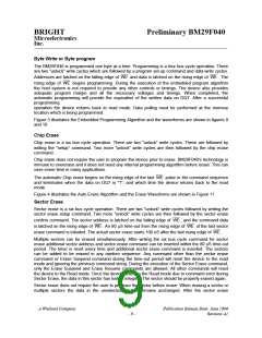
Byte Write or Byte program
The BM29F040 is programmed one byte at a time. Programming is a four bus cycle operation. There
are two "unlock" write cycles which are followed by a program set-up command and data write cycles.
Addresses are latched on the falling edge of WE and data is latched on the rising edge of WE . The
rising edge of WE begins programming. During the execution of the embedded program algorithm
the host system is not required to provide any other controls or timings. The device also provides
adequate program margin and all the necessary voltages and timings. When completed, the
automatic programming will provide the equivalent of the written data on DQ7. After a successful
programming
operation the device returns back to read mode. Data polling must be performed at the memory
location which is being programmed.
Figure 3 illustrates the Embedded Programming Algorithm and the waverforms are shown in figures 9
and 10.
Chip Erase
Chip erase is a six bus cycle operation. There are two "unlock" write cycles. These are followed by
writing the ²setup² command. Two more "unlock" write cycles are then followed by the chip erase
command.
Chip erase does not require the user to program the device prior to erase. BM29F040's technology is
immune to overerase and it does not need any internal programming algorithm before erase. This can
save erase time in many applications.
The automatic Chip erase begins on the rising edge of the last WE pulse in the command sequence
and terminates when the data on DQ7 is "1", and which time the device returns back to the read
mode.
Figure 4 illustrates the Auto Erase Algorithm and the Erase Waveforms are shown in Figure 11.
Sector Erase
Sector erase is a six bus cycle operation. There are two "unlock" write cycles followed by writing the
sector erase setup command. Two more "unlock" write cycles are then followed by the sector erase
confirm command. The sector address is latched on the failing edge of WE , and the command data
is latched on the rising edge of WE . An 80 mS time-out from the rising edge of WE of the last sector
erase command is initiated. The actual sector erase starts 100 uS after the last rising edge of WE .
Multiple sectors can be erased simultaneously. After writing the six bus cycle command for sector
erase additional sector address and sector erase command can be inserted within the 80 uS time-out
period. The timer is reset every time and additional sector erase command is inserted. The sectors
can be added to be erased in any random sequence. Any command other than the sector erase
command or Erase Suspend command during the time-out period will reset the device to the read
mode and ignoring the previous command string. During the execution of the Sector Erase command,
only the Erase Suspend and Erase Resume commands are allowed. All other commands will reset
the device to the Read mode. Once the device resets to the Read mode due to command error during
Sector Erase, the data in this sector has lost its integrity. The sector should be properly erased again.
Sector erase does not require the user to program the sector before erase. When erasing a sector or
multiple sectors the data in the unselected sectors remains unchanged. After the sector erase
A Winbond Company
Publication Release Date: June 1999
Revision A1
- 9 -

 WINBOND [ WINBOND ]