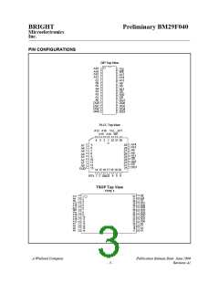
BRIGHT
Microelectronics
Inc.
Preliminary BM29F040
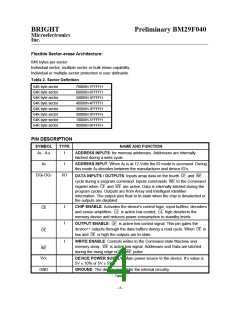
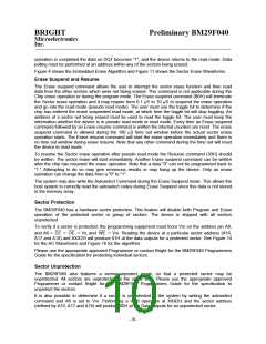
Autoselect Mode
The Autoselect mode allows access to the manufacturers and the device code. This mode can be
enabled by either taking the address pin A9 to VID (11.5 to 12.5 volts) or by giving the Autoselect
Command sequence as shown in Table 5. Once the Autoselect mode is enabled two identifier bytes
can be read on the device outputs by toggling A0 from VIL to VIH. Byte 0 (A0 = VIL) represents the
manufacturers code (ADH for BMI). Byte 1 (A0 = VIH) represents the device identifier and this is 40H
for the BM29F040. A READ command must be written to the Command register to return to the Read
mode after the Autoselect mode.
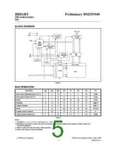
Write Operations
The on-chip state machines control the Chip Erase, Sector Erase and byte Write operations. This
frees the system processor to do other tasks. All the Programming and Erase voltages are generated
internally. The Write and Erase timings and algorithms are also built into the device. The byte write/
sector erase or Chip Erase Command Interface provides additional data protection to avoid
accidental Write or Erase.
Commands are written to the Command register using standard microprocessor write timings. The
Command register recognizes Read mode, Autoselect mode, Chip Erase, Sector Erase (64K bytes
per sector) and Program commands. The Command register does not occupy an addressable
memory location. The interface register is a latch used to store the command and address and data
information needed to execute the command.
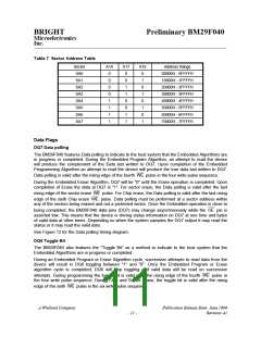
Command Definitions
Device operations are selected by writing specific address and data sequences into the Command
register. Table 6 defines these Command sequences.
Read/ Reset Command
The read or reset operation is initiated by writing the read/reset command sequence to the command
register. Processor read cycles retrieve the data from the memory. The device remains enabled for
reads until the command register contents are changed.
The device will automatically power-up in the read/reset mode. In this case, a command sequence is
not needed to read the memory data. This default power up to read mode ensures that no spurious
changes of the data can take place during power-up. As shown in this data sheet, the timing
parameters and A.C. read waveforms should be referenced.
A single cycle reset is also available as shown in table.
A Winbond Company
Publication Release Date: June 1999
Revision A1
- 7 -

 WINBOND [ WINBOND ]