FEDL87V2107-01
OKI Semiconductor
ML87V2107
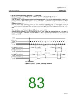
3.1.4 Composite Sync. Signal Internal Generation Timing
For output of the OHS pin, composite SYNC can be selected.
In composite Sync. signal mode, SVD[7:0], SHW[7:0], and VSYM cannot be set.
• Composite Sync. Signal Horizontal Direction Timing
Table F3-1-4(1) Horizontal Direction Timing (VMD[1:0] = 0h:1H = 64 µs)
HMD
A
4.7 µs
63
B
59.3 µs
801
C
2.35 µs
32
D
29.65 µs
400
E
27.3 µs
369
F
4.7 µs
63
[0]
0
[1]
0
1
0
69
875
35
437
403
69
0
1
69
875
35
437
403
69
1
1
—
—
—
—
—
—
* In Flicker Free and Progressive mode, the number of pixels remains unchanged, however, the time cycle
becomes 1/2 (unit: µs).
Table F3-1-4(2) Horizontal Direction Timing (VMD[1:0] = 1h:1H = 63.556 µs)
HMD
A
4.7 µs
63
B
58.856 µs
795
C
2.3 µs
31
D
E
F
4.7 µs
63
[0]
0
[1]
0
29.478 µs 27.078 µs
398
362
422
—
366
333
388
—
1
0
57
723
28
57
0
1
67
843
33
67
1
1
—
—
—
—
* In Flicker Free and Progressive mode, the number of pixels remains unchanged, however, the time cycle
becomes 1/2 (unit: µs).
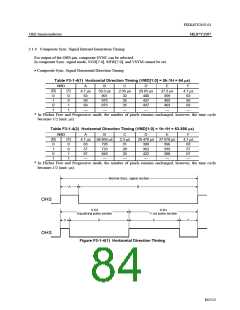
Normal Sync. signal section
A
B
OHS
OHS
0.5H
0.5H
Equalizing pulse section
V cut pulse section
C
D
E
F
Figure F3-1-4(1) Horizontal Direction Timing
84/152

 OKI [ OKI ELECTRONIC COMPONETS ]