FEDL87V2107-01
OKI Semiconductor
ML87V2107
3.2 Sync. Signal Adjustment
3.2.1 OVS, OHS Pin Output Polarity Setting
The Sync. signals that are output from the OVS and OHS pins are of the normal polarity. However, if Sync.
signals of a negative polarity are required, Sync. signals of a negative polarity can be output by setting I2C-bus
setting registers OVSINV and OHSINV.
Table F3-2-1 OVS, OHS Pin Output Polarity (INT = 1 or IINT = 1)
OVSINV
OHSINV
OVS
Positive output
Negative output
—
OHS
—
0
1
X
X
0
1
—
X
X
Positive output
Negative output
—
3.2.2 OHS Pin Output Signal Setting
This IC allows selection of horizontal Sync. signal or composite SYNC for output of the OHS pin by setting the
I2C-bus setting register HSSEL(SUB:68h-bit[3]).
When SMD=1 is set, there are no equalization pulses in composite SYNC.
Table F3-2-2 OHS Pin Output
HSSEL
OHS Pin Output
0
1
Horizontal Sync. signal
Composite Sync. signal
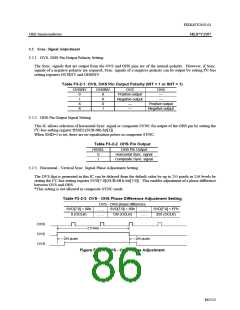
3.2.3 Horizontal - Vertical Sync. Signal Phase Adjustment Setting
The OVS that is generated in this IC can be delayed from the default value by up to 255 pixels in 256 levels by
setting the I2C-bus setting register SVD[7:0](SUB:6B h-bit[7:0]). This enables adjustment of a phase difference
between OVS and OHS.
*This setting is not allowed in composite SYNC mode.
Table F3-2-3 OVS - OHS Phase Difference Adjustment Setting
OVS - OHS phase difference
SVD[7:0] = 00h
0 (OCLK)
SVD[7:0] = 80h
128 (OCLK)
SVD[7:0] = FFh
255 (OCLK)
……
……
……
……
OHS
OVS
OVS
2.5 lines
255 pixels
255 pixels
Figure F3-2-3 OVS - OHS Phase Adjustment
86/152

 OKI [ OKI ELECTRONIC COMPONETS ]