FEDL87V2107-01
OKI Semiconductor
ML87V2107
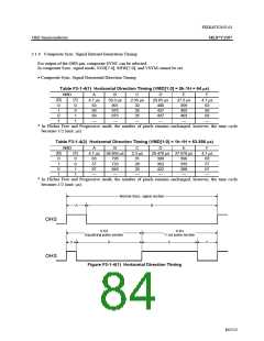
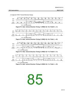
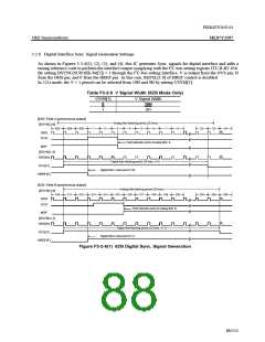
3.2.6 Digital Interface Sync. Signal Generation Settings
As shown in Figures 3-2-6(1), (2), (3), and (4), this IC generates Sync. signals for digital interface and adds a
timing reference code to perform the interface output complying with the I2C-bus setting register ITU-R BT.656.
By setting DSYNC(SUB:6Eh-bit[7]) = 1 through the I2C-bus setting interface, V is output from the OVS pin, H
from the OHS pin, and F from the HREF pin. In this case, REFSL[1:0] of HREF control is disabled.
In 525i mode, the V = 1 period can be selected from 19H and 9H by setting VSYM[1].
Table F3-2-6 V Signal Width (525i Mode Only)
VSYM[1]
V Signal Width
0
19H
1
9H
[625i: Field A synchronous output]
[DSYNC=0]
Analog field blanking period (25 lines)
623
624
625
1
2
3
4
5
6
7
8
22
23
24
OHS
OVS
Field detection point of analog field A
#OF
[DSYNC=1]
OHS(H)
Digital field blanking period (24 lines: V=1)
OVS(V)
Digital field 1 start point (F=0)
HREF(F)
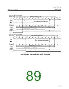
[625i: Field B synchronous output]
[DSYNC=0]
Analog field blanking period (25 lines)
315 316 317 318 319
310
311
312
313
314
320
334
335
336
OHS
OVS
Field detection point of analog field B
#OF
[DSYNC=1]
OHS(H)
Digital field blanking period (25 lines: V=1)
OVS(V)
Digital field 2 start point (F=1)
HREF(F)
Figure F3-2-6(1) 625i Digital Sync. Signal Generation
88/152

 OKI [ OKI ELECTRONIC COMPONETS ]