FEDL87V2107-01
OKI Semiconductor
ML87V2107
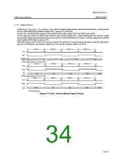
1.3.2 Output Data Format
The output of this IC complies with 16-bit 4:2:2 (YI[7:0] = Y-8bit, CI[7:0] = CbCr-8bit 4:2:2) format (16-bit
output mode), 8-bit 4:2:2 (YI[7:0] = YCbCr-8bit 4:2:2, without SAV, EVA) format (8-bit output mode) and
ITU-R BT.656 conforming (YI[7:0] = YCbCr-8bit 4:2:2, with SAV, EAV) format (ITU-R BT.656 output mode).
The output format mode is set by an external pin MODE 4, MODE 5, or I2C-bus setting register DOSEL
(SUB:60h-bit[1]), or R656O (SUB:60h-bit[2]).
Switching of an external pin and a register is accomplished by setting the I2C-bus setting register IRMON
(SUB:40h-bit[7]).
However, if the Sync. signal generation mode is set inactive, the 8-bit output mode and the ITU-R BT.656 output
mode cannot be selected.
In 8-bit output mode and ITU-R BT.656 output mode, the CO[7:0] that is not used is placed in Hi-Z.
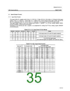
Table F1-3-1(1) Output Data Format Mode
IRMON
MODE4
MODE5
DOSEL
R656O
Mode
0
1
0
1
0
1
0
X
1
X
X
0
X
0
X
X
X
0
16-bit output mode
X
1
8-bit output mode
X
1
X
1
X
1
X
1
ITU-R BT.656 output mode
(SAV and EAV addition)
X
X
Table F1-3-2 (1) Output Data Format
Output
YO7
YO6
YO5
YO4
YO3
YO2
YD1
YD0
CO7
CO6
CO5
CO4
CO3
CO2
CO1
CO0
Normal mode
8-bit input – 8-bit output mode (DOSEL =1)
Y07
Y06
Y07
Y06
Cr07
Cr06
Cr05
Cr04
Cr03
Cr02
Cr01
Cr00
—
Y17
Y16
Y15
Y14
Y13
Y12
Y11
Y10
—
Cb07
Cb06
Cb05
Cb04
Cb03
Cb02
Cb01
Cb00
—
Y17
Y16
Y15
Y14
Y13
Y12
Y11
Y10
—
Y05
Y05
Y04
Y04
Y03
Y03
Y02
Y02
Y01
Y01
Y00
Y00
Cb07
Cb06
Cb05
Cb04
Cb03
Cb02
Cb01
Cb00
Cr07
Cr06
Cr05
Cr04
Cr03
Cr02
Cr01
Cr00
—
—
—
—
—
—
—
—
—
—
—
—
—
—
—
—
—
—
—
—
—
—
—
—
—
—
—
—
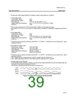
16-bit output mode
OCLK
8-bit output or ITU-R BT.656 output mode
OCLK
#OOCLK
#OOCLK
Yn
Cn
Yn+1
Cn+1
Yn+2
Cn+2
Yn+3
Cn+3
Cbn
Yn
Crn
Yn+1
YO[7:0]
CO[7:0]
YO[7:0]
CO[7:0]
Hi-Z
#: Internal signal
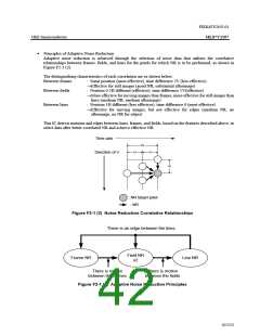
Figure F1-3-2(1) Output Data Timing
38/152

 OKI [ OKI ELECTRONIC COMPONETS ]