FEDL674000-02
OKI Semiconductor
ML674000
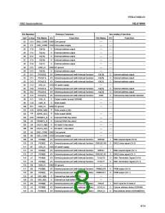
Primary/
Secondary
Pin Name
I/O
Description
Logic
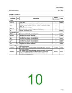
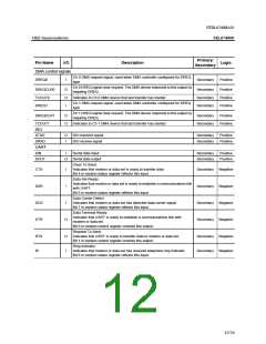
DMA control signals
Ch 0 DMA request signal, used when DMA controller configured for DREQ
type
DREQ0
I
Secondary
Positive
Ch 0 DREQ signal clear request. The DMA device responds to this output by
negating DREQ.
DREQCLR0
TCOUT0
DREQ1
O
O
I
Secondary
Secondary
Secondary
Positive
Positive
Positive
Indicates to Ch 0 DMA device that last transfer has started
Ch 1 DMA request signal, used when DMA controller configured for DREQ
type
Ch 1 DREQ signal clear request. The DMA device responds to this output by
negating DREQ.
DREQCLR1
O
O
Secondary
Secondary
Positive
Positive
TCOUT1
SIO
Indicates to Ch 1 DMA device that last transfer has started
STXD
SRXD
UART
SIN
O
I
SIO transmit signal
SIO receive signal
Secondary
Secondary
Positive
Positive
I
Serial data input
Serial data output
Secondary
Secondary
Positive
Positive
SOUT
O
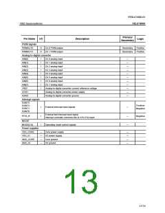
Clear To Send.
Indicates that modem or data set is ready to transfer data.
Bit 4 in modem status register reflects this input.
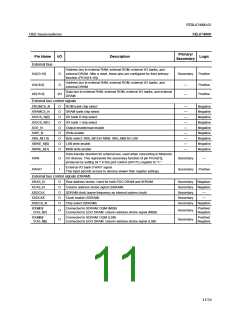
CTS
DSR
DCD
DTR
I
I
Secondary Negative
Secondary Negative
Secondary Negative
Secondary Negative
Data Set Ready.
Indicates that modem or data set is ready to establish a communications link
with UART.
Bit 5 in modem status register reflects this input.
Data Carrier Detect.
Indicates that modem or data set has detected data carrier signal.
Bit 7 in modem status register reflects this input.
Data Terminal Ready.
Indicates that UART is ready to establish a communications link with
modem or data set.
Bit 0 in modem control register controls this output.
I
O
Request To Send.
Indicates that UART is ready to transfer data to modem or data set.
Bit 1 in modem control register controls this output.
RTS
RI
O
I
Secondary Negative
Secondary Negative
Ring Indicator.
Indicates that modem or data set has received telephone ring indicator.
Bit 6 in modem status register reflects this input.
12/24

 OKI [ OKI ELECTRONIC COMPONETS ]