FEDL674000-02
OKI Semiconductor
ML674000
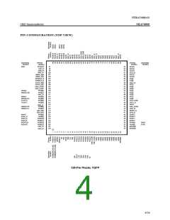
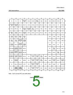
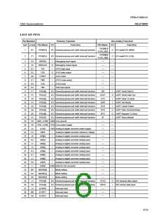
Pin Number
Primary Function
Function
Secondary Function
Pin Name I/O Function
TQFP LFBGA Pin Name I/O
82
83
G13 GND_CORE GND Core ground
VDD_CORE VDD Core power supply
—
—
—
—
—
—
—
—
—
XA[19]
XA[20]
XA[21]
—
XA[22]
XA[23]
XWR
—
—
—
—
—
—
—
—
—
—
O
F11
F10
F12
E12
F13
E10
D12
E13
E11
D11
D13
C12
D10
B12
A12
A11
C10
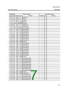
84
XA[13]
XA[14]
O
O
O
O
O
External address output
External address output
External address output
External address output
External address output
85
86
XA[15]
87
XA[16]
88
XA[17]
89
GND_IO
XA[18]
GND I/O ground
90
O
External address output
91
PIOA[10]
PIOA[11]
PIOA[12]
VDD_IO
I/O General-purpose port (with interrupt function)
I/O General-purpose port (with interrupt function)
I/O General-purpose port (with interrupt function)
VDD I/O power supply
External address output
External address output
External address output
92
O
93
O
94
—
O
95
PIOA[13]
PIOA[14]
PIOA[15]
XOE_N
I/O General-purpose port (with interrupt function)
I/O General-purpose port (with interrupt function)
I/O General-purpose port (with interrupt function)
External address output
96
O
External address output
97
O
External bus data transfer direction
98
O
O
Output enable (except SDRAM)
Write enable
—
—
—
99
XWE_N
—
—
100
101
102
103
104
105
106
107
108
109
110
111
112
113
114
115
116
117
118
119
120
121
122
123
B11
A10
C9
GND_IO
XBWE_N[0]
XBWE_N[1]
XROMCS_N
XRAMCS_N
XIOCS_N[0]
XIOCS_N[1]
GND I/O ground
O
Write enable (LSB)
O
Write enable (MSB)
—
—
—
—
—
—
—
DREQ0
—
—
—
—
—
—
—
I
B10
A9
D9
B9
A8
B8
D8
C8
B7
D7
C7
A7
C6
D6
B6
B5
A6
D5
B4
A5
C5
O
O
O
O
External ROM chip select
External RAM chip select
I/O bank 0 chip select
I/O bank 1 chip select
GND_CORE GND Core ground
VDD_CORE VDD Core power supply
PIOB[0]
PIOB[1]
VDD_IO
PIOB[2]
PIOB[3]
PIOB[4]
PIOB[5]
GND_IO
PIOB[6]
PIOB[7]
XBS_N[0]
XBS_N[1]
PIOB[8]
PIOB[9]
PIOB[10]
I/O General-purpose port (with interrupt function)
DMA request signal (Ch 0)
DREQ clear signal (Ch 0)
I/O General-purpose port (with interrupt function) DREQCLR0
O
VDD I/O power supply
—
DREQ1
—
I
I/O General-purpose port (with interrupt function)
DMA request signal (Ch 1)
DREQ clear signal (Ch 1)
I/O General-purpose port (with interrupt function) DREQCLR1
O
I/O General-purpose port (with interrupt function)
I/O General-purpose port (with interrupt function)
GND I/O ground
TCOUT0
TCOUT1
—
O
DMA Termination Signal (CH 0)
DMA Termination Signal (CH 1)
O
—
O
I/O General-purpose port (with interrupt function) PWMOUT0
I/O General-purpose port (with interrupt function) PWMOUT1
PWM output (Ch 0)
PWM output (Ch 1)
O
O
O
External bus byte select (LSB)
External bus byte select (MSB)
—
—
XWAIT
XCAS_N
XRAS_N
—
—
I
I/O General-purpose port (with interrupt function)
I/O General-purpose port (with interrupt function)
I/O General-purpose port (with interrupt function)
WAIT input for IO bank 0
O
Column address strobe (SDRAM)
Row address strobe (SDRAM/EDO)
O
8/24

 OKI [ OKI ELECTRONIC COMPONETS ]