FEDL674000-02
OKI Semiconductor
ML674000
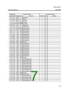
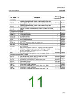
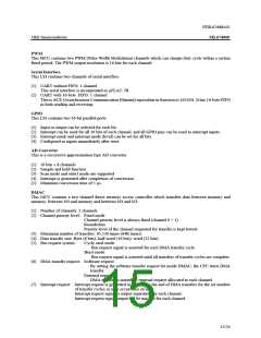
Primary/
Secondary
Pin Name
I/O
Description
Logic
External Bus
Address bus to external RAM, external ROM, external I/O banks, and
external DRAM. After a reset, these pins are configured for their primary
function (PIOA[14:10]).
XA[23:19]
O
Secondary
Positive
Address bus to external RAM, external ROM, external I/O banks, and
external DRAM
Data bus to external RAM, external ROM, external I/O banks, and external
DRAM
XA[18:0]
XD[15:0]
O
—
—
Positive
Positive
I/O
External bus control signals
XROMCS_N
XRAMCS_N
XIOCS_N[0]
XIOCS_N[1]
XOE_N
O
O
O
O
O
O
O
O
O
ROM bank chip select
SRAM bank chip select
I/O bank 0 chip select
I/O bank 1 chip select
Output enable/read enable
Write enable
—
—
—
—
—
—
—
—
—
Negative
Negative
Negative
Negative
Negative
Negative
Negative
Negative
Negative
XWE_N
XBS_N[1:0]
XBWE_N[0]
XBWE_N[1]
Byte select: XBS_N[1] for MSB; XBS_N[0] for LSB
LSB write enable
MSB write enable
Data transfer direction for external bus, used when connecting to Motorola
I/O devices. This represents the secondary function of pin PIOA[15],
produced by setting bit 7 in the port control (GPCTL) register to "1."
External I/O bank 0 WAIT signal.
This input permits access to devices slower than register settings.
XWR
O
Secondary
Secondary
—
XWAIT
I
Positive
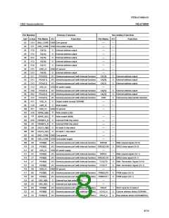
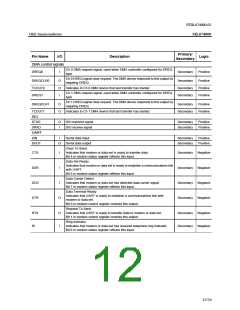
External bus control signals (DRAM)
XRAS_N
XCAS_N
XSDCLK
XSDCKE
XSDCS_N
O
O
O
O
O
Row address strobe. Used for both EDO DRAM and SDRAM.
Column address strobe signal (SDRAM)
SDRAM clock (same frequency as internal system clock)
Clock enable (SDRAM)
Secondary Negative
Secondary Negative
Secondary
Secondary
—
—
Chip select (SDRAM)
Secondary Negative
XDQM[1]/
XCAS_N[1]
Connected to SDRAM: DQM (MSB)
Positive/
O
O
Secondary
Connected to EDO DRAM: column address strobe signal (MSB)
Negative
XDQM[0]/
XCAS_N[0]
Connected to SDRAM: DQM (LSB)
Connected to EDO DRAM: column address strobe signal (LSB)
Positive/
Negative
Secondary
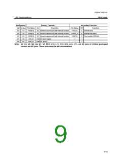
11/24

 OKI [ OKI ELECTRONIC COMPONETS ]