FEDL674000-02
OKI Semiconductor
ML674000
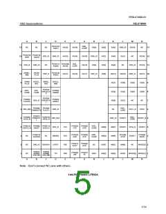
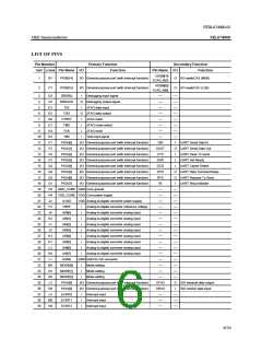
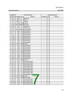
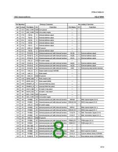
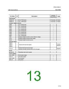
Pin Number
Primary Function
Function
Secondary Function
Pin Name I/O Function
SDRAM clock
TQFP LFBGA Pin Name I/O
124
125
126
127
128
C4
A4
B3
D4
B2
PIOB[11]
PIOB[12]
PIOB[13]
VDD_IO
GND_IO
I/O General-purpose port (with interrupt function)
XSDCLK
O
O
I/O General-purpose port (with interrupt function) XSDCS_N
SDRAM chip select
I/O General-purpose port (with interrupt function)
VDD I/O power supply
XSDCKE
—
O
Clock enable (SDRAM)
—
—
GND I/O ground
—
Note: A1, C3, H2, M2, K6, M7, N7, M12, N13, L11, C13, B13, A13, C11, A3, A2 pins of LFBGA packaged
version are NC pins. These pins must be left unconnected.
9/24

 OKI [ OKI ELECTRONIC COMPONETS ]