EM785830AA
8-bit Micro-controller
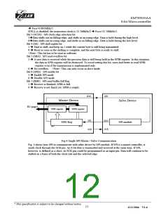
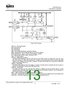
Write
R5
Read
R5
RBF
RBFI
SPIWC
SPIR reg.
SPIW reg.
set to 1
SPIE
Buffer Full Detector
SDI
shift right
SDI/P74
SPIS reg.
MUX
PORT62
bit 7
bit 0
SDO
SPIC reg. (R4 page1)
SDO/P75
MUX
PORT61
Edge
Select
SPIE
0
3
Noise
Filter
SBR2~SBR0
SBR0 ~SBR2
2
3
Clock Select
T
sco
Prescaler
4, 8, 16, 32, 64, 128
SCK
PORT60
Edge
Select
SCK/P76
MUX
16.38kHz
SCK
SPIE
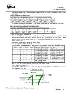
Fig.5 SPI structure
SPIC reg. : SPI control register
SDO: Serial data out
SDI: Serial data in
SCK: Serial clock
RBF : Set by buffer full detector, and reset in software.
RBFI : Interrupt flag. Set by buffer full detector, and reset in software.
Buffer Full Detector : Sets to 1, while an 8-bit shifting is complete.
SE : Loads the data in SPIW register, and begin to shift
SPIE : SPI control register
SPIS reg. : Shifting byte out and in.
The MSB will be shifted first. Both the SPIS register and the SPIW register are loaded at the same time. Once
data being written to, SPIS starts transmission / reception. The received data will be moved to the SPIR
register, as the shifting of the 8-bit data is complete. The RBF (Read Buffer Full ) flag and the RBFI(Read
Buffer Full Interrupt) flag are set.
SPIR reg. : Read buffer.
The buffer will be updated as the 8-bit shifting is complete. The data must be read before the next reception is
finished. The RBF flag is cleared as the SPIR register read.
SPIW reg. : Write buffer.
The buffer will deny any write until the 8-bit shifting is complete. The SE bit will be kept in 1 if the
communication is still under going. This flag must be cleared as the shifting is finished. Users can determine if
the next write attempt is available.
SBR2 ~ SBR0: Programming the clock frequency/rates and sources.
Clock select : Selecting either the internal instruction clock or the external 16.338KHz clock as the shifting clock.
Edge Select : Selecting the appropriate clock edges by programming the SCES bit
__________________________________________________________________________________________________________________________________________________________________
* This specification is subject to be changed without notice.
11
12/1/2004 V1.6

 ELAN [ ELAN MICROELECTRONICS CORP ]