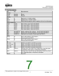
EM785830AA
8-bit Micro-controller
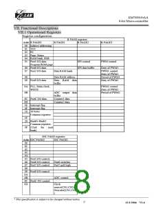
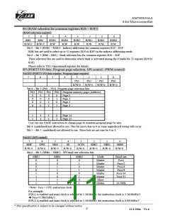
R4 (RAM selection for common registers R20 ~ R3F))
(RAM selection register)
7
6
5
4
3
2
1
0
RB1
RB0
RSR5
R/W
RSR4
R/W
RSR3
R/W
RSR2
R/W
RSR1
R/W
RSR0
R/W
R/W-0
R/W-0
Bit 0 ~ Bit 5 (RSR0 ~ RSR5) : Indirect addressing for common registers R20 ~ R3F
RSR bits are used to select up to 32 registers (R20 to R3F) in the indirect addressing mode.
Bit 6 ~ Bit 7 (RB0 ~ RB1) : Bank selection bits for common registers R20 ~ R3F
These selection bits are used to determine which bank is activated among the 4 banks for 32 register (R20 to
R3F).
Please refer to VII.1 Operational registers for details.
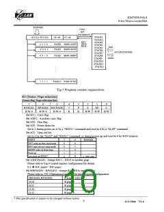
R5 (PORT5 I/O data, Program page selection, SPI control , PWM control)
PAGE0 (PORT5 I/O data register, Program page register)
7
-
6
-
5
-
4
-
3
2
1
0
PS3
PS2
PS1
PS0
R/W-0
R/W-0
R/W-0
R/W-0
Bit 0 ~ Bit 3 (PS0 ~ PS3): Program page selection bits
PS3 PS2 PS1 PS0 Program memory page (Address)
0
0
0
0
:
0
0
0
0
:
0
0
1
1
:
0
1
0
1
:
Page 0
Page 1
Page 2
Page 3
:
:
:
:
:
:
1
1
1
1
1
1
0
1
Page 14
Page 15
User can use PAGE instruction to change page to maintain program page by user.
Bit 4: (undefined) not allowed to use. This bit must clear to 0 or some unpredicted wrong will occur.
Bit 5 ~ Bit 7: (undefined) not allowed to use. These bits are not sure be 0 or 1.
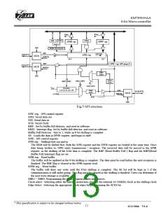
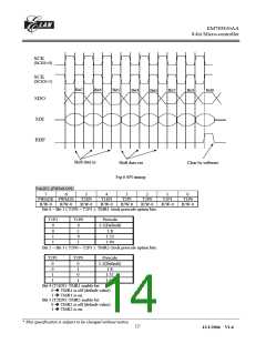
PAGE2 (SPI control)
7
6
5
4
3
2
1
0
RBF
SPIE
SRO
SE
SCES
SBR2
SBR1
SBR0
R/W-0
R/W-0
R/W-0
R/W-0
R/W-0
R/W-0
R/W-0
R/W-0
Bit 0 ~ Bit 2 (SBR0 ~ SBR2) : SPI baud rate selection bits
SBR2
SBR1
SBR0
Mode
Baud rate
Fsco
Fsco/2
Fsco/4
Fsco/8
Fsco/16
Fsco/32
0
0
0
0
1
1
1
1
0
0
1
1
0
0
1
1
0
1
0
1
0
1
0
1
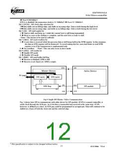
Master
Master
Master
Master
Master
Master
Slave
Master
16.384k
<Note> Fsco = CPU instruction clock
For example :
If PLL is enabled and main clock is selected to 3.5826MHz, the instruction clock is 3.5826MHz/2
Î Fsco=3.5862MHz/2
If PLL is enabled and main clock is selected to 3.5826MHz, the instruction clock is 0.895MHz/2
__________________________________________________________________________________________________________________________________________________________________
* This specification is subject to be changed without notice.
9
12/1/2004 V1.6

 ELAN [ ELAN MICROELECTRONICS CORP ]