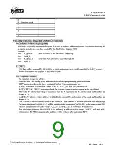
EM785830AA
8-bit Micro-controller
Î Fsco=0.895MHz/2
If PLL is disabled, the instruction clock is 32.768kHz/2 Î Fsco=32.768kHz/2.
Bit 3 (SCES) : SPI clock edge selection bit
1ÎData shifts out on falling edge, and shifts in on rising edge. Data is hold during the high level.
0ÎData shifts out on rising edge, and shifts in on falling edge. Data is hold during the low level.
Bit 4 (SE) : SPI shift enable bit
1 Î Start to shift, and keep on 1 while the current byte is still being transmitted.
0 Î Reset as soon as the shifting is complete, and the next byte is ready to shift.
<Note> This bit has to be reset in software.
Bit 5 (SRO) : SPI read overflow bit
1 Î A new data is received while the previous data is still being hold in the SPIB register. In this situation,
the data in SPIS register will be destroyed. To avoid setting this bit, users had better to read SPIB
register even if the transmission is implemented only.
0 Î No overflow, <Note> This can only occur in slave mode.
Bit 6 (SPIE) : SPI enable bit
1 Î Enable SPI mode
0 Î Disable SPI mode
Bit 7 (RBF) : SPI read buffer full flag
1 Î Receive is finished, SPIB is full.
0 Î Receive is not finish yet, SPIB is empty.
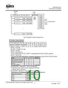
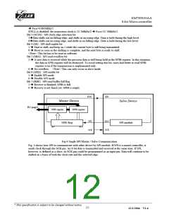
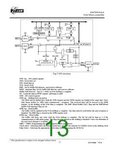
SDO
SDI
Master Device
Salve Device
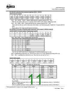
R5 page1
SPIR register
SPIW register
SDI
SDO
SCK
SPI module
SPIS Reg
Bit 0
Bit7
SCK
Fig.4 Single SPI Master / Salve Communication
Fig. 4 shows how SPI to communicate with other device by SPI module. If SPI is a master controller, it
sends clock through the SCK pin. An 8-bit data is transmitted and received at the same time. If SPI,
however, is defined as a slave, its SCK pin could be programmed as an input pin. Data will continue to be
shifted on a basis of both the clock rate and the selected edge.
__________________________________________________________________________________________________________________________________________________________________
* This specification is subject to be changed without notice.
10
12/1/2004 V1.6

 ELAN [ ELAN MICROELECTRONICS CORP ]