EM785830AA
8-bit Micro-controller
VII. Functional Descriptions
VII.1 Operational Registers
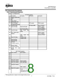
Register configuration
R PAGE registers
R PAGE2
Addr R PAGE0
00 Indirect addressing
01 TCC
R PAGE1
R PAGE3
02 PC
03 Page, Status
04 RAM bank, RSR
05 Port5 I/O data,
Program ROM page
06 Port6 I/O data
07 Port7 I/O data
SPI control
PWM control
SPI data buffer
Duty of PWM1
PWM1 control
Duty of PWM1
Data RAM bank
08
Data RAM address
Data RAM data
buffer
Period of PWM1
Duty of PWM2
09 Port9 I/O data
0A PLL, Main clock,
WDTE
0B
PWM2 control
Duty of PWM2
Period of PWM2
ADC output data
buffer
0C PortC I/O data
0D
Counter1 data
Counter2 data
0E Interrupt flag
0F Interrupt flag
10 16 bytes
:
Common registers
1F
20 Bank0~Bank3
Common registers
:
3F (32x8 for each
bank)
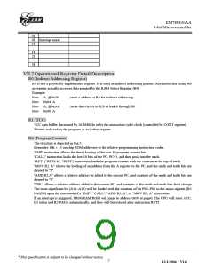
IOC PAGE registers
Addr IOC PAGE0
IOC PAGE1
00
01
02
03
04
05 Port5 I/O control,
06 Port6 I/O control
07 Port7 I/O control
Port6 switches
Port7 pull high
08
09 Port9 I/O control
0A
0B
ADC control
0C PortC I/O control
0D
Clock
source(CN1,CN2)
Prescaler(CN1,CN2
)
__________________________________________________________________________________________________________________________________________________________________
* This specification is subject to be changed without notice.
6
12/1/2004 V1.6

 ELAN [ ELAN MICROELECTRONICS CORP ]