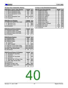
VT82C686B
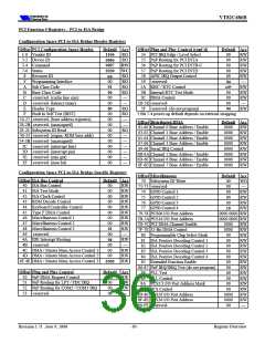
PCI Function 0 Registers – PCI-to-ISA Bridge
Configuration Space PCI-to-ISA Bridge Header Registers
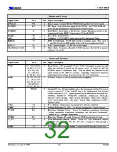
Offset PCI Configuration Space Header
1-0 Vendor ID
3-2 Device ID
5-4 Command
7-6 Status
Default Acc
Offset Plug and Play Control (cont’d)
54 PCI IRQ Edge / Level Select
55 PnP Routing for PCI INTA
56 PnP Routing for PCI INTB-C
57 PnP Routing for PCI INTD
58 APIC IRQ Output Control
59 -reserved-
5A KBC / RTC Control
5B Internal RTC Test Mode
5C DMA Control
Default Acc
RO
RO
RW
WC
RO
RO
RO
RO
—
00
00
00
00
00
04
x4†
00
00
00
04
RW
RW
RW
RW
RW
—
RW
RW
RW
—
1106
0686
0087
0200
nn
00
01
06
00
8
9
Revision ID
Programming Interface
Sub Class Code
A
B
C
D
E
F
Base Class Code
-reserved- (cache line size)
-reserved- (latency timer)
Header Type
00
—
5D-5E -reserved-
5F -reserved- (do not program)
† Bit 7-4 power-up default depends on external strapping
RO
RO
—
RW
80
00
00
Built In Self Test (BIST)
10-27 -reserved- (base address registers)
28-2B -reserved- (unassigned)
2F-2C Subsystem ID Read
30-33 -reserved- (expan. ROM base addr)
34-3B -reserved- (unassigned)
3C -reserved- (interrupt line)
3D -reserved- (interrupt pin)
3E -reserved- (min gnt)
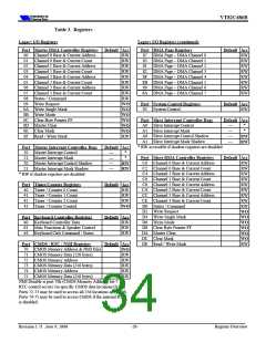
Offset Distributed DMA
Default Acc
00
—
61-60 Channel 0 Base Address / Enable
63-62 Channel 1 Base Address / Enable
65-64 Channel 2 Base Address / Enable
67-66 Channel 3 Base Address / Enable
69-68 Serial IRQ Control
6B-6A Channel 5 Base Address / Enable
6D-6C Channel 6 Base Address / Enable
6F-6E Channel 7 Base Address / Enable
0000
0000
0000
0000
0000
0000
0000
0000
RW
RW
RW
RW
RW
RW
RW
RW
00
00
RO
—
00
—
00
—
00
—
00
—
3F -reserved- (max lat)
00
—
Configuration Space PCI-to-ISA Bridge-Specific Registers
Offset Miscellaneous
70 Subsystem ID Write
71-73 -reserved-
74 GPIO Control 1
75 GPIO Control 2
76 GPIO Control 3
77 GPIO Control 4
Default Acc
Offset ISA Bus Control
Default Acc
00
00
00
00
00
10
WO
—
RW
RW
RW
RW
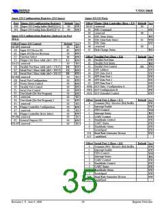
40 ISA Bus Control
41 ISA Test Mode
42 ISA Clock Control
43 ROM Decode Control
44 Keyboard Controller Control
45 Type F DMA Control
46 Miscellaneous Control 1
47 Miscellaneous Control 2
48 Miscellaneous Control 3
49 -reserved-
00
00
00
00
00
00
00
00
RW
RW
RW
RW
RW
RW
RW
RW
RW
—
79-78 PCS0# I/O Port Address
7B-7A PCS1# I/O Port Address
7D-7C PCI DMA Channel Enable
7F-7E 32-Bit DMA Control
80 Programmable Chip Select Mask
81 ISA Positive Decoding Control 1
82 ISA Positive Decoding Control 2
83 ISA Positive Decoding Control 3
84 ISA Positive Decoding Control 4
85 Extended Function Enable
86-87 PnP IRQ/DRQ Test (do not program)
88 PLL Test
89 PLL Control
8A PCS2/3 I/O Port Address Mask
8B PCS Control
8D-8C PCS2# I/O Port Address
8F-8E PCS3# I/O Port Address
90-FF -reserved-
0000 0000 RW
0000 0000 RW
0000
0000
00
00
00
00
00
00
00
00
00
00
00
0000
0000
00
RW
RW
RW
RW
RW
RW
RW
RW
RW
RW
RW
RW
RW
RW
RW
—
01
00
4A IDE Interrupt Routing
4B -reserved-
RW
—
04
00
4C DMA / Master Mem Access Control 1
4D DMA / Master Mem Access Control 2
4F-4E DMA / Master Mem Access Control 3
00
00
0300
RW
RW
RW
Offset Plug and Play Control
50 PnP DMA Request Control
51 PnP Routing for LPT / FDC IRQ
52 PnP Routing for COM2 / COM1 IRQ
53 -reserved-
Default Acc
RW
RW
RW
—
2D
00
00
00
Revision 1.71 June 9, 2000
-30-
Register Overview

 ETC [ ETC ]