VT82C686B
Resets and Clocks
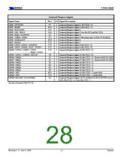
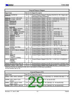
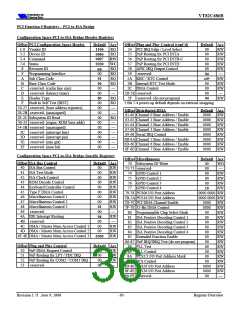
Signal Name
Pin #
I/O Signal Description
W6
B16
I
O
Connected to the PWRGOOD signal on the Power Supply.
PWRGD
PCIRST#
Power Good.
Active low reset signal for the PCI bus. The VT82C686B will
PCI Reset.
assert this pin during power-up or from the control register.
Reset signal to the ISA bus. Connect through an inverter to the
J1
O
RSTDRV
Reset Drive.
chipset north bridge RESET# input and to PCI bus RESET#.
H5
E4
Y5
O
I
I
ISA bus clock.
14.31818 MHz clock signal used by the internal Timer.
BCLK
OSC
RTCX1
Bus Clock.
Oscillator.
: 32.768 KHz crystal or oscillator input. This input is
RTC Crystal Input
used for the internal RTC and for power-well power management logic.
W5
T8
O
O
: 32.768 KHz crystal output
RTC Crystal Output
.Frequency selectable if PMU function 4 Rx54[1-0] is nonzero
Slow Clock.
RTCX2
SLOWCLK
/ GPO0
(set to 01, 10, or 11).
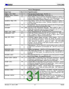
Power and Ground
Signal Name
VCC
Pin #
I/O Signal Description
F7, F10, F12-F14,
H6, H15, J6, J15,
K6, K15, M6,
P
P
P
3.3V nominal (3.15V to 3.45V). This supply is turned on only
Core Power.
when the mechanical switch on the power supply is turned on and the
PWRON signal is conditioned high. This pin should be connected to the
same voltage as the CPU I/O circuitry. Internally connected to hardware
monitoring system voltage detection circuitry for 3.3V monitoring.
M15, N6, N15,
R7-R8, R11, R14
F6, F11, F15, G6,
G15, J9-J12, K9-
K12, L6, L9-L12,
L15, M9-M12,
Connect to primary motherboard ground plane.
GND
Ground.
P6, P15, R6, R15
R9-R10
Always available unless the mechanical switch of the power
VCCS
Suspend Power.
supply is turned off. If the “soft-off” state is not implemented, then this pin
can be connected to VCC. Signals powered by or referenced to this plane are:
PWRGD, RSMRST#, PWRBTN#, SMBCLK, SMBDATA, SUSCLK,
SUSA# / GPO1, SUSB# / GPO2, SUSC#, SUSST1# / GPO6, GPI1 / IRQ8#,
GPI2 / BATLOW#, GPI3 / LID, GPI5 / PME#, GPI6 / SMBALRT#, GPI7 /
RING#, GPO0
Y6
T13
R12
P
P
P
Battery input for internal RTC (RTCX1, RTCX2)
RTC Battery.
VBAT
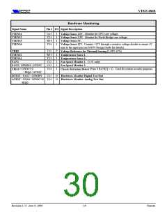
VREF
VCCH
(5V ±5%). For thermal sensing and 5V input tolerance.
Voltage Reference
Power for hardware monitoring subsystem
Hardware Monitor Power.
(voltage monitoring, temperature monitoring, and fan speed monitoring).
Connect to VCC through a ferrite bead.
R13
F9
P
P
Connect to GND through a ferrite bead.
Hardware Monitor Ground.
GNDH
VCCU
Power for USB differential outputs
USB Differential Output Power.
(USBP0+, P0-, P1+, P1-, P2+, P2-, P3+, P3-). Connect to VCC through a
ferrite bead.
F8
P
Connect to GND through a ferrite bead.
USB Differential Output Ground.
GNDU
Revision 1.71 June 9, 2000
-26-
Pinouts

 ETC [ ETC ]