VT82C686B
PCI Function 4 Registers - Power Management
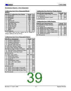
Configuration Space Power Management Header
Registers
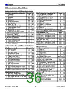
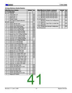
Configuration Space Hardware Monitor Registers
Offset System Management Bus
71-70 Hardware Mon IO Base (128 Bytes)
72-73 -reserved-
Default Acc
0001
00
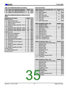
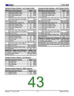
Offset PCI Configuration Space Header
1-0 Vendor ID
3-2 Device ID
5-4 Command
7-6 Status
Default Acc
RW
—
RW
—
RO
RO
RO
WC
RO
RO
RO
RO
RO
RO
RO
RO
—
1106
3057
0000
0280
nn
74 Hardware Monitor Control
75-8F -reserved-
00
00
8
9
Revision ID
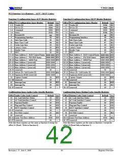
Configuration Space SMBus Registers
Programming Interface
Sub Class Code
Base Class Code
Cache Line Size
Latency Timer
Header Type
A
B
C
D
E
F
Offset System Management Bus
93-90 SMBus I/O Base (16 Bytes)
94-D1 -reserved-
D2 SMBus Host Configuration
D3 SMBus Host Slave Command
D4 SMBus Slave Address Shadow Port 1
D5 SMBus Slave Address Shadow Port 2
D6 SMBus Revision ID
Default Acc
0000 0001
RW
—
00
00
00
00
00
00
nn
00
00
00
00
00
RW
RW
RW
RW
RO
—
BIST
10-3F -reserved-
† The default values for these registers may be changed by
writing to offsets 61-63h (see below).
D7-FF -reserved-
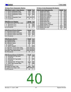
Configuration Space Power Management Registers
Offset Power Management
40 General Configuration 0
41 General Configuration 1
42 ACPI Interrupt Select
43 Internal Timer Read Test
45-44 Primary Interrupt Channel
47-46 Secondary Interrupt Channel
4B-48 Power Mgmt I/O Base (256 Bytes)
4C Host Bus Power Management Control
4D Throttle / Clock Stop Control
4E-4F -reserved-
Default Acc
00
RW
RW
RW
RO
RW
RW
RW
RW
RW
—
00
00
—
0000
0000
0000 0001
00
00
00
53-50 GP Timer Control
0000 0000 RW
54 Power Well Control
55 USB Wakeup Control
56 -reserved-
57 Miscellaneous Control
58 GP2 / GP3 Timer Control
59 GP2 Timer
5A GP3 Timer
5B-60 -reserved-
61 Write value for Offset 9 (Prog Intfc)
62 Write value for Offset A (Sub Class)
63 Write value for Offset B (Base Class)
64-7F -reserved-
00
00
00
00
00
00
00
00
00
00
00
00
RW
RW
—
RW
RW
RW
RW
—
WO
WO
WO
—
Revision 1.71 June 9, 2000
-33-
Register Overview

 ETC [ ETC ]