VT82C686B
REGISTERS
Register Overview
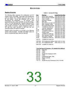
Table 2. System I/O Map
Port
Function
Master DMA Controller
Master Interrupt Controller 0000 0000 001x xxxn
Actual Port Decoding
0000 0000 000x nnnn
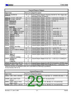
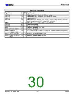
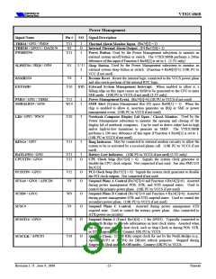
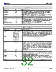
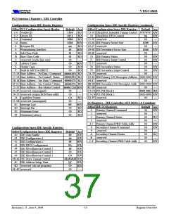
The following tables summarize the configuration and I/O
registers of the VT82C686B. These tables also document the
power-on default value (“Default”) and access type (“Acc”)
for each register. Access type definitions used are RW
(Read/Write), RO (Read/Only), “—” for reserved / used
(essentially the same as RO), and RWC (or just WC) (Read /
Write 1’s to Clear individual bits). Registers indicated as RW
may have some read/only bits that always read back a fixed
value (usually 0 if unused); registers designated as RWC or
WC may have some read-only or read write bits (see
individual register descriptions for details).
00-1F
20-3F
40-5F
60-6F
(60h)
(61h)
(64h)
70-77
78-7F
80
81-8F
90-91
92
93-9F
A0-BF
C0-DF
E0-FF
Timer / Counter
Keyboard Controller
KBC Data
Misc Functions & Spkr Ctrl 0000 0000 0110 xxx1
KBC Command / Status 0000 0000 0110 x1x0
RTC/CMOS/NMI-Disable 0000 0000 0111 0nnn
-available for system use- 0000 0000 0111 1xxx
-reserved- (debug port)
DMA Page Registers
-available for system use- 0000 0000 1001 000x
System Control 0000 0000 1001 0010
-available for system use- 0000 0000 1001 nnnn
Slave Interrupt Controller 0000 0000 101x xxxn
Slave DMA Controller
-available for system use- 0000 0000 111x xxxx
0000 0000 010x xxnn
0000 0000 0110 xnxn
0000 0000 0110 x0x0
0000 0000 1000 0000
0000 0000 1000 nnnn
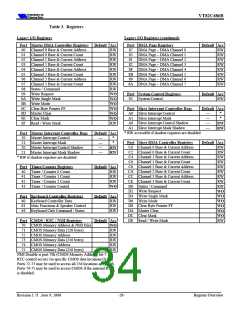
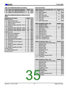
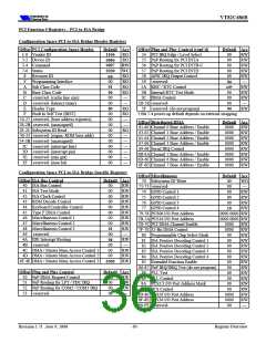
Detailed register descriptions are provided in the following
section of this document. All offset and default values are
shown in hexadecimal unless otherwise indicated
0000 0000 110n nnnx
100-CF7 -available for system use*
CF8-CFB PCI Configuration Address 0000 1100 1111 10xx
CFC-CFF PCI Configuration Data
0000 1100 1111 11xx
D00-FFFF -available for system use-
* On-Chip Super-I/O Functions – PC-Standard Port Addresses
200-20F Game Port
2E8-2EF COM4
2F8-2FF COM2
378-37F
Parallel Port (Standard & EPP)
3E8-3EF COM3
3F0-3F1
3F0-3F7
Configuration Index / Data
Floppy Controller
3F8-3FF COM1
778-77A Parallel Port (ECP Extensions) (Port 378+400)
Revision 1.71 June 9, 2000
-27-
Register Overview

 ETC [ ETC ]