VT82C686B
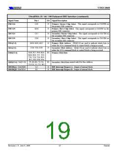
UltraDMA-33 / 66 / 100 Enhanced IDE Interface (continued)
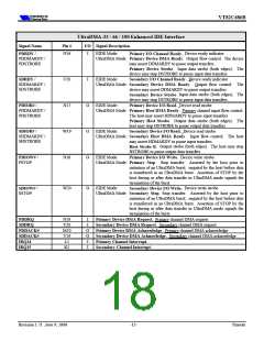
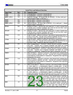
Signal Name
PDCS1#
Pin #
I/O Signal Description
L20
O
O
O
O
O
O
This signal corresponds to CS1FX# on
This signal corresponds to CS3FX# on the
Primary Master Chip Select.
the primary IDE connector.
Primary Slave Chip Select.
primary IDE connector.
M16
U17
PDCS3#
SDCS1#
SDCS3#
PDA[2-0]
SDA[2-0]
PDD[15-0]
This signal corresponds to CS17X# on
This signal corresponds to CS37X# on
Secondary Master Chip Select.
the secondary IDE connector.
Secondary Slave Chip Select.
the secondary IDE connector.
U18
M18, M19, M17
U20, V18, U19
PDA[2:0] are used to indicate which byte in
Primary Disk Address.
either the ATA command block or control block is being accessed.
SDA[2:0] are used to indicate which byte in
Secondary Disk Address.
either the ATA command block or control block is being accessed.
N20, P17, P19, R16, IO
R18, R20, T17, T19,
T20, T18, T16, R19,
R17, P20, P18, P16
Primary Disk Data
/ SA[15-0]
P5, R1-R5, T1-T4,
U1-U3, V1, V2, W1
IO
muxed with ISA Bus Address.
Secondary Disk Data
SDD[15-0]
/ DACK0#
/ DACK1#
L2
E1
O
O
Output of internal block.
Output of internal block.
IDEIRQA
IDEIRQB
IDE Interrupt Request A.
IDE Interrupt Request B.
Revision 1.71 June 9, 2000
-13-
Pinouts

 ETC [ ETC ]