VT82C686B
Pin Descriptions
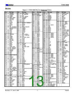
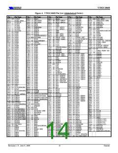
Table 1. Pin Descriptions
PCI Bus Interface
Signal Name
Pin #
I/O Signal Description
(see pin list)
IO
IO
IO
The standard PCI address and data lines. The address is driven with
FRAME# assertion and data is driven or received in following cycles.
AD[31:0]
C/BE[3:0]#
FRAME#
Address/Data Bus.
C19, F17,
G20, J19
F18
The command is driven with FRAME# assertion. Byte enables
Command/Byte Enable.
corresponding to supplied or requested data are driven on following clocks.
Assertion indicates the address phase of a PCI transfer. Negation indicates that
Frame.
one more data transfer is desired by the cycle initiator.
F19
F20
G17
G16
IO
IO
IO
IO
Asserted when the initiator is ready for data transfer.
Asserted when the target is ready for data transfer.
Asserted by the target to request the master to stop the current transaction.
IRDY#
TRDY#
STOP#
Initiator Ready.
Target Ready.
Stop.
The VT82C686B asserts this signal to claim PCI transactions through
DEVSEL#
Device Select.
positive or subtractive decoding. As an input, DEVSEL# indicates the response to a
VT82C686B-initiated transaction and is also sampled when decoding whether to
subtractively decode the cycle.
G19
G18
IO
I
A single parity bit is provided over AD[31:0] and C/BE[3:0]#.
Parity.
PAR
SERR#
SERR# can be pulsed active by any PCI device that detects a system error
System Error.
condition. Upon sampling SERR# active, the VT82C686B can be programmed to
generate an NMI to the CPU.
C20
I
I
IDSEL is used as a chip select during configuration read and
write cycles. Connect this pin to AD18 using a 100 Ω resistor.
IDSEL
Initialization Device Select.
A16, D17,
C17, B17
. These pins are typically connected to the PCI bus INTA#-
PIRQA-D#
PCI Interrupt Request
INTD# pins as follows:
PIRQA#
PIRQB#
INTB#
INTC#
INTD#
INTA#
PIRQC#
INTC#
INTD#
INTA#
INTB#
PIRQD#
INTD#
INTA#
INTB#
INTC#
PCI Slot 1
PCI Slot 2
PCI Slot 3
PCI Slot 4
INTA#
INTB#
INTC#
INTD#
L18
L19
O
I
This signal goes to the North Bridge to request the PCI bus.
This signal is driven by the North Bridge to grant PCI access to the
PREQ#
PGNT#
PCI Request.
PCI Grant.
VT82C686B.
E16
I
PCLK provides timing for all transactions on the PCI Bus.
PCI Clock.
PCLK
W12
IO
This signal indicates whether the PCI clock is or will be stopped
PCI Bus Clock Run.
PCKRUN#
(high) or running (low). The VT82C686B drives this signal low when the PCI clock is
running (default on reset) and releases it when it stops the PCI clock. External devices
may assert this signal low to request that the PCI clock be restarted or prevent it from
stopping. Connect this pin to ground using a 100 Ω resistor if the function is not used.
Refer to the “PCI Mobile Design Guide” and the VIA “Apollo MVP4 Design Guide” for
more details.
B16
O
Active low reset signal for the PCI bus. The VT82C686B will assert this pin
PCIRST#
PCI Reset.
during power-up or from the control register.
Revision 1.71 June 9, 2000
-9-
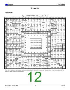
Pinouts

 ETC [ ETC ]