VT82C686B
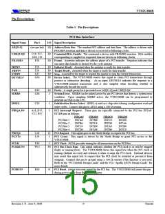
CPU Interface
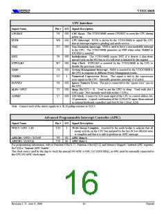
Signal Name
CPURST
Pin # I/O Signal Description
V8
W8
U7
OD
OD
OD
The VT82C686B asserts CPURST to reset the CPU during
CPU Reset.
power-up.
INTR is driven by the VT82C686B to signal the CPU
INTR
NMI
CPU Interrupt.
that an interrupt request is pending and needs service.
Non-Maskable Interrupt.
NMI is used to force a non-maskable interrupt
to the CPU. The VT82C686B generates an NMI when either SERR# or
IOCHK# is asserted.
T6
W7
U6
V7
Y8
T7
OD
OD
OD
I
The VT82C686B asserts INIT if it detects a shut-down
INIT
Initialization.
special cycle on the PCI bus or if a soft reset is initiated by the register
STPCLK# is asserted by the VT82C686B to the CPU to
Stop Clock.
STPCLK#
SMI#
throttle the processor clock.
SMI# is asserted by the VT82C686B to
System Management Interrupt.
the CPU in response to different Power-Management events.
This signal is tied to the coprocessor
FERR#
IGNNE#
Numerical Coprocessor Error.
error signal on the CPU. Internally generates interrupt 13 if active.
OD
OD
OD
This pin is connected to the “ignore error” pin on
Ignore Numeric Error.
the CPU.
/ GPO7
(Rx75[7] = 0). Used to put the CPU to sleep. Used with slot-1
SLP#
A20M#
Sleep
CPUs only. Not currently used with socket-7 CPUs.
Connect to A20 mask input of the CPU to control address bit-
Y7
A20 Mask.
20 generation. Logical combination of the A20GATE input (from internal
or external keyboard controller) and Port 92 bit-1 (Fast_A20).
Note: Connect each of the above signals to 4.7K Ω pullup resistors to VCC3.
Advanced Programmable Interrupt Controller (APIC)
Signal Name
Pin # I/O Signal Description
U10
/ GPI3 / LID
I
Asserted by the north bridge to indicate that all
Write Snoop Complete.
WSC#
snoop activity on the CPU bus initiated by the last PCI-to-DRAM write
is complete and that it is safe to perform an APIC interrupt.
/ GPO1 / SUSA#
/ SUSCLK
V9
T10
IO
IO
APICD0
APICD1
APIC Data 0.
APIC Data 1.
For programming information, refer to Function 0 Rx74,77, Function 4 Rx54[3-2], and Memory Mapped / Indexed APIC registers.
Rx77[4] is “Internal APIC Enable”.
The clock source used by the chip to clock the internal I/O APIC is OSC (14.31818 MHz), so OSC must be externally connected to
the CPU I/O APIC clock input.
Revision 1.71 June 9, 2000
-10-
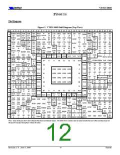
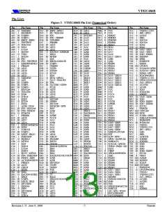
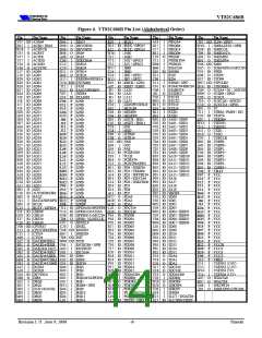
Pinouts

 ETC [ ETC ]