VT82C686B
Universal Serial Bus Interface
Signal Name
Pin # I/O Signal Description
A3
B3
C4
D4
A4
B4
B5
E6
C3
G5
IO
IO
IO
IO
IO
IO
IO
IO
I
USBP0+
USBP0-
USBP1+
USBP1-
USBP2+
USBP2-
USBP3+
USBP3-
USBCLK
USB Port 0 Data +
USB Port 0 Data -
USB Port 1 Data +
USB Port 1 Data -
USB Port 2 Data +
USB Port 2 Data -
USB Port 3 Data +
USB Port 3 Data -
48MHz clock input for the USB interface
USB Clock.
/ GPO25 / DACK2# / FDCIRQ
I
Port 0 is disabled if low.
USBOC0#
USB Port 0 Over Current Detect.
USBOC0# if Rx76[7] = 1 and Rx76[6] = 0
/ GPO24 / DRQ2 / FDCDRQ
/ SERIRQ
H3
I
Port 1 is disabled if this input
USB Port 1 Over Current Detect.
USBOC1#
is low. Direct inputs are provided for overcurrent protection for
ports 0 and 1 which may be used if the alternate functions of these
two pins are not required. If overcurrent protection is desired on all
four ports (or it is desired to use the alternate functions of these two
pins), an external buffer may be used to drive the state of
USBOC[3-0]# onto SD[3-0] during ISA bus refresh cycles (i.e.,
while ISA bus RFSH# is low, so that RFSH# may be used as the
buffer enable). USCOC1# if Rx76[7] = 1 and Rx76[6] = 0.
(SD2 & RFSH#)
(SD1 & RFSH#)
(SD0 & RFSH#)
(SD3 & RFSH#)
(W2)
(Y2)
(Y1)
(Y3)
I
I
I
I
USBOC0#
USBOC1#
USBOC2#
USBOC3#
USB Port 0 Over Current Detect
USB Port 1 Over Current Detect
USB Port 2 Over Current Detect
USB Port 3 Over Current Detect
/ DACK6#
/ DACK7#
M3
N2
O
O
Output of internal block.
Output of internal block.
USBIRQA
USBIRQB
USB Interrupt Request A.
USB Interrupt Request B.
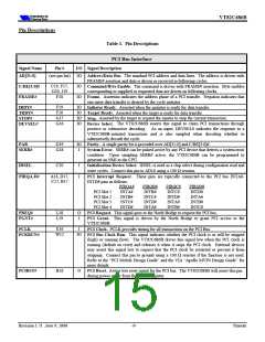
System Management Bus (SMB) Interface (I2C Bus)
Signal Name
Pin # I/O Signal Description
U9
T9
W10
IO
IO
I
SMBCLK
SMBDATA
SMBALRT#
SMB / I2C Clock.
SMB / I2C Data.
/ GPI6
(System Management Bus I/O space Rx08[3] = 1)
SMB Alert.
When the chip is enabled to allow it, assertion generates an IRQ or
SMI interrupt or a power management resume event. The same pin
is used as General Purpose Input 6 whose value is reflected in
Rx48[6] of function 4 I/O space
Revision 1.71 June 9, 2000
-11-
Pinouts

 ETC [ ETC ]