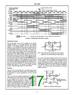
ICL7104
the Auto-Zero and wait for Run/Hold to go high. As above, the MODE input is high, the chip and byte ENABLE termi-
Integrate (Phase II) begins seven clock periods after the nals become TTL-compatible outputs which provide the con-
high level is detected.
trol signals for the output cycle. The Send ENABLE pin
(SEN) (pin 29) is used as an indication of the ability of the
external device to receive data. The condition of the line is
sensed once every clock pulse, and if it is high, the next (or
first) byte is enabled on the next rising CLOCK 1 (pin 25)
clock edge, the corresponding byte ENABLE line goes low,
and the CHIP ENABLE / LOAD pin (pin 30) (CE/LD) goes
low for one full clock pulse only, returning high.
Direct Mode
When the MODE pin is left at a low level, the data outputs
[bits 1 through 8 low order byte, See Table 3 for format of
middle (-16) and high order bytes] are accessible under
control of the byte and CHIP ENABLE terminals as inputs.
These ENABLE inputs are all active low, and are provided
with pullup resistors to ensure an inactive high level when
left open. When the CHIP ENABLE input is low, taking a
byte ENABLE input low will allow the outputs of that byte to
become active (three-stated on). This allows a variety of
parallel data accessing techniques to be used. The timing
requirements for these outputs are shown under AC
Specifications and Table 1.
On the next falling CLOCK 1 clock pulse edge, if SEN
remains high, or after it goes high again, the byte output
lines will be put in the high impedance state (or three-stated
off). One half pulse later, the byte ENABLE pin will be
cleared high, and (unless finished) the CE/LD and the next
byte ENABLE pin will go low. This will continue until all three
(2 in the case of the 14-bit device) bytes have been sent.
The bytes are individually put into the low impedance state
i.e.: three-stated on during most of the time that their byte
ENABLE pin is (active) low. When receipt of the last byte
has been acknowledged by a high SEN, the handshake
mode will be cleared, re-enabling data latching from conver-
sion, and recognizing the condition of the MODE pin again.
The byte and CHIP ENABLE will be three-stated off, if
MODE is low, but held by their (weak) pullups. These timing
relationships are illustrated in Figures 11, 12, and 13, and
Table 2.
It should be noted that these control inputs are asynchro-
nous with respect to the converter clock - the data may be
accessed at any time. Thus it is possible to access the data
while it is being updated, which could lead to scrambled
data. Synchronizing the access of data with the conversion
cycle by monitoring the STATUS output will prevent this.
Data is never updated while STATUS is low. Also note the
potential bus conflict described under “Initial Clear Circuitry”.
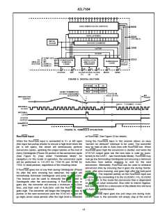
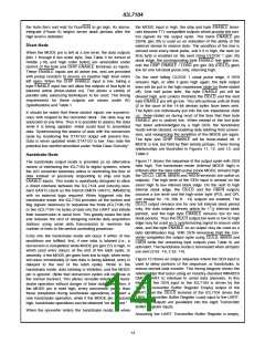
Handshake Mode
Figure 11 shows the sequence of the output cycle with SEN
held high. The handshake mode (Internal MODE high) is
entered after the data latch pulse (since MODE remains high
the CE/LD, LBEN, MBEN and HBEN terminals are active as
outputs). The high level at the SEN input is sensed on the
same high to low internal clock edge. On the next to high
internal clock edge, the CE/LD and the HBEN outputs
assume a low level and the high-order byte (POL and OR,
and except for -16, Bits 9 - 14) outputs are enabled. The
The handshake output mode is provided as an alternative
means of interfacing the ICL7104 to digital systems, where
the A/D converter becomes active in controlling the flow of
data instead of passively responding to chip and byte
ENABLE inputs. This mode is specifically designed to allow
a direct interface between the ICL7104 and industry-stan-
dard UARTs (such as the Intersil CMOS UARTs, IM6402/3)
with no external logic required. When triggered into the
handshake mode, the ICL7104 provides all the control and
flag signals necessary to sequence the three (ICL7106-16)
or two (ICL7104-14) bytes of data into the UART and initiate
their transmission in serial form. This greatly eases the task
and reduces the cost of designing remote data acquisition
stations using serial data transmission to minimize the
number of lines to the central controlling processor.
CE/LD output remains low for one full internal clock period
1
only, the data outputs remain active for 1 / internal clock
2
periods, and the high byte ENABLE remains low for two
clock periods. Thus the CE/LD output low level or low to high
edge may be used as a synchronizing signal to ensure valid
data, and the byte ENABLE as an output may be used as a
byte identification flag. With SEN remaining high the con-
verter completes the output cycle using CE/LD, MBEN and
LBEN while the remaining byte outputs (see Table 3) are
activated. The handshake mode is terminated when all bytes
are sent (3 for -16, 2 for -14).
Entry into the handshake mode will occur if either of two
conditions are fulfilled; first, if new data is latched (i.e., a
conversion is completed) while MODE pin (pin 27) is high, in
which case entry occurs at the end of the latch cycle; or
secondly, if the MODE pin goes from low to high, when entry
will occur immediately (if new data is being latched, entry is
delayed to the end of the latch cycle). While in the
handshake mode, data latching is inhibited, and the MODE
pin is ignored. (Note that conversion cycles will continue in
the normal manner). This allows versatile initiation of hand-
shake operation without danger of false data generation; if
the MODE pin is held high, every conversion (other than
those completed during handshake operations) will start a
new handshake operation, while if the MODE pin is pulsed
high, handshake operations can be obtained “on demand.”
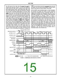
Figure 12 shows an output sequence where the SEN input is
used to delay portions of the sequence, or handshake, to
ensure correct data transfer. This timing diagram shows the
relationships that occur using an industry-standard IM6402/3
CMOS UART to interface to serial data channels. In this
interface, the SEN input to the ICL7104 is driven by the
TBRE (Transmitter Buffer Register Empty) output of the
UART, and the CE/LD terminal of the ICL7104 drives the
TBRL (Transmitter Buffer Register Load) input to the UART.
The data outputs are paralleled into the eight Transmitter
Buffer Register inputs.
When the converter enters the handshake mode, or when
Assuming the UART Transmitter Buffer Register is empty,
14

 ETC [ ETC ]