ICL7104
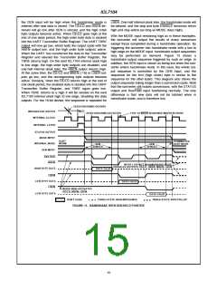
the SEN input will be high when the handshake mode is LBEN. One-half internal clock later, the handshake mode will
entered after new data is stored. The CE/LD and HBEN ter- be cleared, and the chip and byte ENABLE terminals return
minals will go low after SEN is sensed, and the high order high and stay active (as long as MODE stays high).
byte outputs become active. When CE/LD goes high at the
With the MODE input remaining high as in these examples,
end of one clock period, the high order byte data is clocked
the converter will output the results of every conversion
into the UART Transmitter Buffer Register. The UART TBRE
except those completed during a handshake operation. By
output will now go low, which halts the output cycle with the
triggering the converter into handshake mode with a low to
HBEN output low, and the high order byte outputs active.
high edge on the MODE input, handshake output sequences
When the UART has transferred the data to the Transmitter
may be performed on demand. Figure 13 shows
a
Register and cleared the Transmitter Buffer Register, the
TBRE returns high. On the next ICL7104 internal clock high
to low edge, the high order byte outputs are disabled, and
one-half internal clock later, the HBEN output returns high.
At the same time, the CE/LD and MBEN (-16) or LBEN out-
puts go low, and the corresponding byte outputs become
active. Similarly, when the CE/LD returns high at the end of
one clock period, the enabled data is clocked into the UART
Transmitter Buffer Register, and TBRE again goes low.
When TBRE returns to a high it will be sensed on the next
ICL7104 internal clock high to low edge, disabling the data
outputs. For the 16-bit device, the sequence is repeated for
handshake output sequence triggered by such an edge. In
addition, the SEN input is shown as being low when the con-
verter enters handshake mode. In this case, the whole out-
put sequence is controlled by the SEN input, and the
sequence for the first (high order) byte is similar to the
sequence for the other bytes. This diagram also shows the
output sequence taking longer than a conversion cycle. Note
that the converter still makes conversions, with the STATUS
output and Run/Hold input functioning normally. The only
difference is that new data will not be latched when in
handshake mode, and is therefore lost.
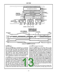
ZERO-CROSSING OCCURS
INTEGRATOR OUTPUT
ZERO-CROSSING DETECTED
FOR -16 MBEN SEQUENCE INSERTED HERE
INTERNAL CLOCK
INTERNAL LATCH
STATUS OUTPUT
MODE INPUT
UART
TERMINATES
UART MODE
INTERNAL MODE
NORM
SEN
SENSED
SEN
SENSED
SEN INPUT
CE/LOAD
HBEN
MODE LOW NOT IN HANDSHAKE MODE
DISABLES OUTPUTS CE/LD, HBEN, MBEN, LBEN
HIGH BYTE DATA
DATA VALID
LBEN
LOW BYTE DATA
LBEN
DATA VALID
MODE HIGH ACTIVATES
CE/LD, HBEN, LBEN
LOW BYTE DATA
DATA VALID
THREE-STATE WITH PULLUP
DON’T CARE
THREE-STATE HIGH IMPEDANCE
FIGURE 11. HANDSHAKE WITH SEN HELD POSITIVE
15

 ETC [ ETC ]