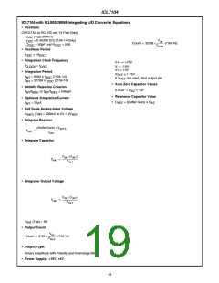
ICL7104
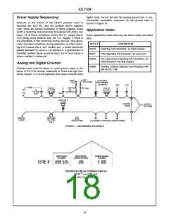
digital loads are not fed into the analog ground line. A rec-
ommended connection sequence for the ground lines is
shown in Figure 16.
Power Supply Sequencing
Because of the nature of the CMOS process used to
fabricate the ICL7104, and the multiple power supplies
used, there are certain conditions of these supplies under
which a disabling and potentially damaging SCR action can
occur. All of these conditions involve the V+ supply (Norm
+5V) being more positive than the V++ supply. If there is
any possibility of this occurring during start-up, shut down,
under transient conditions during operation, or when insert-
ing a PC board into a “hot” socket, etc., a diode should be
placed between V+ and V++ to prevent it. A germanium or
Schottky rectifier diode would be best, but in most cases a
silicon rectifier is adequate.
Application Notes
Some application notes that may be found useful are listed
here:
NOTE #
AN016
AN017
AN018
DESCRIPTION
“Selecting A/D Converters”, by Dave Fullagar
“The Integrating A/D Converter”, by Lee Evans
“Do’s and Don’ts of Applying A/D Converters,” by
Peter Bradshaw and Skip Osgood
Analog and Digital Grounds
AN030
“Building a Battery-Operated Auto Ranging DVM
with the ICL7106”
Extreme care must be taken to avoid ground loops in the
layout of ICL7104 circuits, especially in 16-bit and high sen-
sitivity circuits. It is most important that return currents from
REF
VOLTAGE
BUFF
OUT
EXTERNAL
REFERENCE
(IF USED)
+15V
-15V
BUFF
-IN
(IF USED)
V
PIN 35
ICL7104
AN GND
PIN 35
ICL7104
AN GND
REF
I/P
FILTER
CAP
+
V
C
IN
-
AZ
8068 PIN 2
COMP
BOARD
EDGE
SUPPLY
RETURN
DIGITAL
LOGIC
DIG GND
ICL7104
PIN 2
DEVICE PIN
+5V SUPPLY BYPASS CAPACITOR(S)
FIGURE 1. GROUNDING SEQUENCE
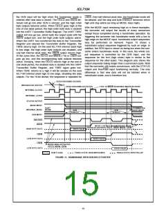
AUTOZERO
(COUNT)
INTEGRATE
(FIXED COUNT)
DEINTEGRATE
(COUNT)
IC L7 104 - 14
IC L7 104 - 16
24,576 - 8,193
98,304 - 32,769
8192
32768
0 - 16383
0 - 65535
CONVERSION TIME (IN CONTINUOUS MODE):
†
32,768 tO SC (7104 - 14)
†
131,072 tO SC (7104 - 16)
18

 ETC [ ETC ]