ICL7104
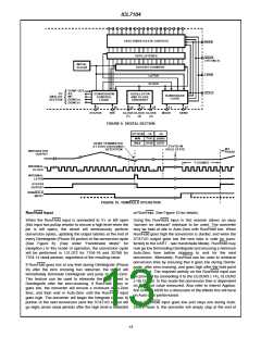
POSITIVE TRANSITION
CAUSES ENTRY INTO
UART MODE
ZERO-CROSSING OCCURS
ZERO-CROSSING DETECTED
INTERNAL
CLOCK
LATCH PULSE INHIBITED
IN UART MODE
INTERNAL
LATCH
STATUS OUTPUT UNAFFECTED
BY UART MODE
STATUS
OUTPUT
DEINT PHASE III
MODE
INPUT
UART
INTERNAL
NORM
MODE
SEN INPUT
CE/LOAD
AS OUTPUT
HBEN
HIGH BYTE
DATA
DATA VALID
MBEN
MIDDLE
DATA VALID
BYTE DATA
LBEN
LOW BYTE
DATA
DATA VALID
DON’T CARE
THREE-STATE HIGH IMPEDANCE
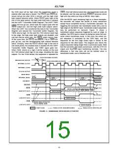
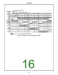
FIGURE 13. HANDSHAKE TRIGGERED BY MODE
THREE-STATE WITH PULLUP
Initial Clear Circuitry
The internal logic of the 7104 is supplied by an internal
regulator between V++ and Digital Ground. The regulator
includes a low-voltage detector that will clear various
registers. This is intended to ensure that on initial power-up,
the control logic comes up in Auto-Zero, with the 2nd, 3rd,
and 4th MSB bits cleared, and the “mode” F/F cleared (i.e.,
in “direct” mode). This, however, will also clear these regis-
ters if the supply voltage “glitches” to a low enough value.
Additionally, if the supply voltage comes up too fast, this
clear pulse may be too narrow for reliable clearing. In gen-
eral, this is not a problem, but if the UART internal “MODE”
F/F should come up set, the byte and chip ENABLE lines will
become active outputs. In many systems this could lead to
bus conflicts, especially in non-handshake systems. In any
case, SEN should be high (held high for non-handshake sys-
tems) to ensure that the MODE F/F will be cleared as fast as
possible (see Figure 11 for timing). For these and other
reasons, adequate supply bypass is recommended.
25
24
26
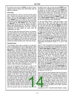
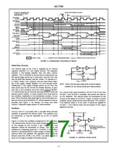
R
CLOCK
1
CLOCK
2
CLOCK
3
C
f
= 0.45/RC
OSC
NOTE: Clock 3 has the same output drive as the bit outputs.
FIGURE 14. RC OSCILLATOR (ICL7104-14 ONLY)
As a result of pin count limitations, the ICL7104-16 has only
CLOCK 1 and CLOCK 2 available, and cannot be used as
an RC oscillator. The internal clock will correspond to the
inverse of the signal on CLOCK 2. Figure 15 shows a crystal
oscillator circuit, which can be used with both 7104 versions.
If an external clock is to be used, it should be applied to
CLOCK 1. This internal clock will correspond to the signal
applied to this pin.
Oscillator
The ICL7104-14 is provided with a versatile three terminal
oscillator to generate the internal clock. The oscillator may
be overdriven, or may be operated as an RC or crystal
oscillator.
V+
Figure 14 shows the oscillator configured for RC operation.
The internal clock will be of the same frequency and phase
as the voltage on the CLOCK 3 pin. The resistor and
capacitor should be connected as shown. The circuit will
oscillate at a frequency given by f = 0.45/RC. A 50 - 100kΩ
resistor is recommended for useful ranges of frequency. For
optimum 60Hz line rejection, the capacitor value should be
chosen such that 32768 (-16), 8192 (-14) clock periods is
close to an integral multiple of the 60Hz period.
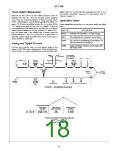
25
26
CLOCK
1
CLOCK
2
†CAPACITOR VALUE
DEPENDS ON CRYSTAL
TYP 0-30pF
†
CRYSTAL
FIGURE 15. CRYSTAL OSCILLATOR
17

 ETC [ ETC ]