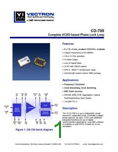
CD-700, VCXO Based PLL
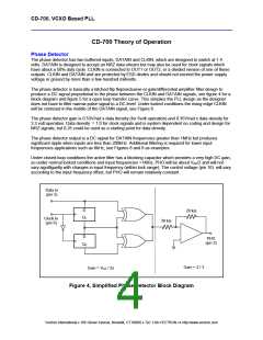
Phase Detector
CD-700 Theory of Operation
The phase detector has two buffered inputs, DATAIN and CLKIN, which are designed to switch at 1.4
volts. DATAIN is designed to accept an NRZ data stream but may also be used for clock signals which
have about a 50% duty cycle. CLKIN is connected to OUT1 or OUT2, or a divided version of one of these
outputs. CLKIN and DATAIN and are protected by ESD diodes and should not exceed the power supply
voltage or ground by more than a few hundred millivolts.
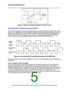
The phase detector is basically a latched flip flop/exclusive-or gate/differential amplifier filter design to
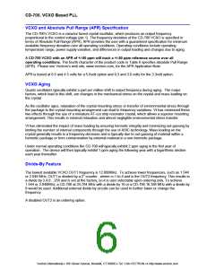
produce a DC signal proportional to the phase between the CLKIN and DATAIN signals, see figure 4 for a
block diagram and figure 5 for a open loop transfer curve. This simplies the PLL design as the designer
does not have to filter narrow pulse signal to a DC level. Under locked conditions the rising edge CLKIN
will be centered in the middle of the DATAIN signal, see Figure 6.
The phase detector gain is 0.53V/rad x data density (for 5volt operation) and 0.35V/rad x data density for
3.3 volt operation. Data density = 1.0 for clock signals and is system dependent on coding and design for
NRZ signals, but 0.25 could be used as a starting point for data density.
The phase detector output is a DC signal for DATAIN frequencies greater than 1MHz but produces
significant ripple when inputs are less than 200kHz. Additional filtering is required for lower input
frequencies applications such as 8kHz, see Figures 8 and 9 as examples.
Under closed loop conditions the active filter has a blocking capacitor which provides a very high DC gain,
so under normal locked conditions and input frequencies >1MHz, PHO will be about VDD/2 and will not
vary signifigantly with changes in input frequency (within lock range). The control voltage (pin 16) will vary
according to the input frequency offset, but PHO will remain relatively constant.
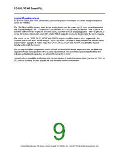
Data In
(pin 5)
D
20 kΩ
Q1
Clock In
(pin 6)
30 kΩ
D
PHO
(pin 3)
Q2
Gain = 2 / 3
Gain = VDD / 2π
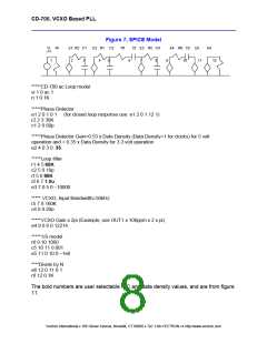
Figure 4, Simplified Phase Detector Block Diagram
Vectron International • 166 Glover Avenue, Norwalk, CT 06856 • Tel: 1-88-VECTRON-1• http://www.vectron.com

 ETC [ ETC ]