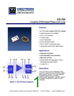
CD-700, VCXO Based PLL
Performance Characteristics
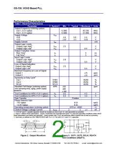
Table 1. Electrical Performance
Parameter
Symbol
Min
Typical
Maximum
Units
Output Frequency (ordering option)
Out 1, 5.0 V option
Out 1, 3.3 V option
Supply Voltage 1
12.000
12.000
65.536
51.840
MHz
MHz
VDD
+5.0
+3.3
4.5
2.97
5.0
3.3
5.5
3.63
V
V
Supply Current
IDD
mA
Output Logic Levels
Output Logic High2
Output Logic Low2
Output Transition Times
Rise Time2
VOH
VOL
2.5
V
V
0.5
tR
tF
5
5
ns
ns
Fall Time2
Input Logic Levels
Output Logic High2
Output Logic Low2
Loss of Signal Indication
Output Logic High2
Output Logic Low2
Nominal Frequency on Loss of Signal
Output 1
VIH
VIL
2.0
2.5
V
V
0.5
0.5
VOH
VOL
V
V
ppm
ppm
±75
±75
Output 2
Symmetry or Duty Cycle3
Out 1
Out 2
RCLK
SYM1
SYM2
RCLK
APR
40/60
45/55
40/60
%
%
%
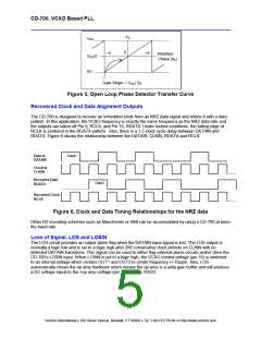
Absolute Pull Range (ordering option)
over operating temp, aging, power supply
variations
ppm
±50
±80
±100
0.5
Test Conditions for APR (+5.0 V option)
Test Conditions for APR (+3.3 V option)
Gain Transfer
VC
VC
4.5
3.0
V
V
0.3
Positive
Phase Detector Gain
+5V option
+3.3V Option
Operating temperature (ordering option)
0.53
0.35
0/70 or –40/85
rad/V
rad/V
°C
Control Voltage Leakage Current
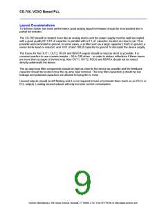
1. A 0.01uF and 0.1 parallel capacitor should be located as close to pin 14 (and grounded) as possible.
IVCXO
uA
±1
2. Figure 1 defines these parameters. Figure 2 illustrates the equivalent five gate TTL load and operating conditions under which
these parameters are tested and specified. Loads greater than 15 pF will adversely effect rise/fall time as well as symmetry.
3. Symmetry is defined as (ON TIME/PERIOD with Vs=1.4 V for both 5.0 V and 3.3 V operation.
TF
TR
IDD
650Ω
80%
1.4V
14
16
+
-
VDD
1µF
.
.01µF
7
20%
IC
VC
On Time
15pF
1.8k
+
-
Period
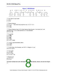
Figure 2. Output Waveform
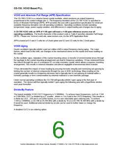
Figure 3. OUT1, OUT2, RCLK, RDATA
Test Conditions (25±5°C)
Vectron International 166 Glover Avenue, Norwalk CT 06856-5160
Tel:1-88-VECTRON-1
e-mail: vectron@vectron.com

 ETC [ ETC ]