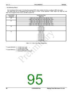
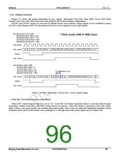
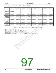
Ver 1.3
PRELIMINARY
EAGLE
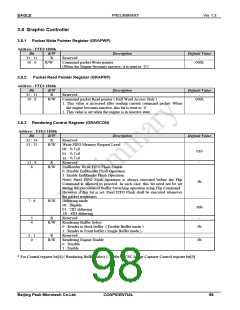
3.8.4 Current Display Bank Register (GRACDB)
Address : FFE0 180Ch
Bit
31 : 25
24
R/W
R
R
Description
Default Value
Reserved
-
Rendering Engine Idle Status
0 : Busy Status
1 : Idle Status
1b
23 : 18
17 : 16
15 : 10
9 : 8
7 : 2
1 : 0
R
R
R
R
R
R
Reserved
Current Rendering Bank
Reserved
Current Display Bank
Reserved
Current Display Bank ( = Frame Front buffer )
-
10b
-
01b
-
00b
3.8.5 Flip Command Count Register (GRAFCC)
Address : FFE0 1810h
Bit
31 : 8
7 : 0
R/W
R
R/W
Description
Default Value
Reserved
Flip Command Count
-
00h
Write ‘0’: Clear the value of this register to ‘0’.
Write ‘1’: Increment the value of this register by 1.
When a Flip Command is executed, the value of this register is
decremented by 1.
Note: During set-up of packet sync flip command, bank switch is executed on the falling edge of vertical sync signal.
For better system performance, this register should be read using video vertical sync interrupt source instead of using register
polling method.
3.8.6 Non-Texture Memory Mode Register (GRANONTEXTURE)
Address : FFE0 1814h
Bit
31 : 1
0
R/W
R
R/W
Description
Default Value
Reserved
-
0b
Non-Texture Memory Mode
0: Using Texture Memory
1: Non-Texture Memory Mode
Note: When this bit is configured as Non-Texture Memory Mode, Texture Memory becomes part of main memory. In this
case, it must be set texture start address register in memory controller.
99
CONFIDENTIAL
Beijing Peak Microtech Co.Ltd.

 ETC [ ETC ]