NCP1271
43 mVńms
8.1 mAńms
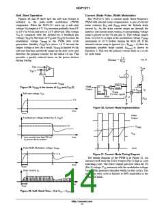
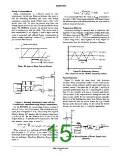
Ramp Compensation
R
+
+ 5.3 kW
(eq. 4)
ramp
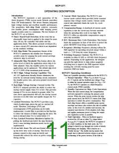
Ramp compensation is a known mean to cure
subharmonic oscillations. These oscillations take place at
half the switching frequency and occur only during
continuous conduction mode (CCM) with a duty−cycle
greater than 50%. To lower the current loop gain, one
usually injects between 50 and 75% of the inductor down
slope. The NCP1271 generates an internal current ramp
that is synchronized with the clock. This current ramp is
then routed to the CS pin. Figures 32 and 33 depict how the
ramp is generated and utilized. Ramp compensation is
It is recommended that the value of R
be limited to
ramp
less then 10 kW. Values larger than this will begin to limit
the effective duty cycle of the controller and may result in
reduced transient response.
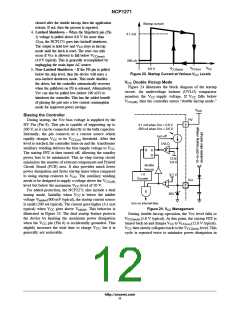
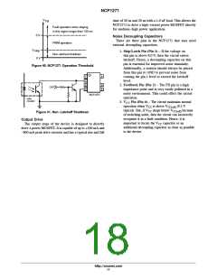
Frequency Jittering
Frequency jittering is a method used to soften the EMI
signature by spreading the energy in the vicinity of the main
switching component. The NCP1271 switching frequency
ranges from +7.5% to −7.5% of the switching frequency in
a linear ramp with a typical period of 6 ms. Figure 34
demonstrates how the oscillation frequency changes.
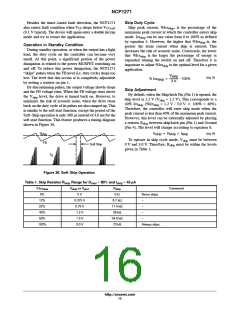
simply formed by placing a resistor, R
pin and the sense resistor.
, between the CS
ramp
Ramp current, I
ramp
Oscillator Frequency
100uA
107.5 kHz
100 kHz
time
0
92.5 kHz
80% of period
100% of period
6 ms
Figure 32. Internal Ramp Current Source
time
Figure 34. Frequency Jittering
(The values are for the 100 kHz frequency option)
DRIVE
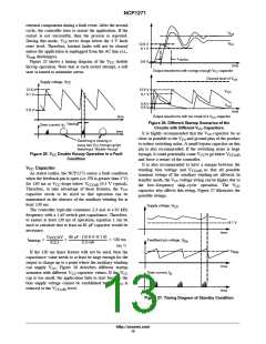
Fault Detection
Figure 35 details the timer−based fault detection
circuitry. When an overload (or short circuit) event occurs,
the output voltage collapses and the optocoupler does not
Clock
100 mA Peak
conduct current. This opens the FB pin (pin 2) and V is
FB
Current
Ramp
R
ramp
CS
internally pulled higher than 3.0 V. Since (V /3) is greater
FB
than 1 V, the controller activates an error flag and starts a
130 ms timer. If the output recovers during this time, the
timer is reset and the device continues to operate normally.
However, if the fault lasts for more than 130 ms, then the
Oscillator
R
sense
driver turns off and the device enters the V
Hiccup mode discussed earlier. At the end of the double
hiccup, the controller tries to restart the application.
Double
CC
Figure 33. Inserting a Resistor in Series with the
Current Sense Information brings Ramp Compensation
For the NCP1271, the current ramp features a swing of
100 mA. Over a 65 kHz frequency with an 80% max duty
cycle, that corresponds to an 8.1 mA/ms ramp. For a typical
flyback design, let’s assume that the primary inductance
(Lp) is 350 mH, the SMPS output is 19 V, the Vf of the
output diode is 1 V and the Np:Ns ratio is 10:1. The OFF
time primary current slope is given by:
4.8V
V
FB
FB 2
V
FB
3
Np
Ns
(Vout ) Vf) @
Fault
+
−
130ms
delay
+ 571 VńmH + 571 mAńms
disable Drv
(eq. 3)
Lp
V
SS
&
When projected over an Rsense of 0.1 W (for example),
this becomes or 57 mV/ms. If we select 75% of the
downslope as the required amount of ramp compensation,
Softstart
1V max
Figure 35. Block Diagram of Timer−Based Fault
then we shall inject 43 mV/ms. Therefore, R
is simply
ramp
Detection
equal to:
http://onsemi.com
14

 ETC [ ETC ]