NCP1271
cleared after the double hiccup, then the application
restarts. If not, then the process is repeated.
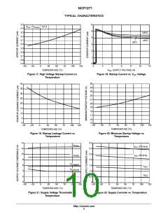
Startup current
4. Latched Shutdown – When the Skip/latch pin (Pin
1) voltage is pulled above 8.0 V for more than
13 ms, the NCP1271 goes into latchoff shutdown.
4.1 mA
The output is held low and V stays in hiccup
CC
mode until the latch is reset. The reset can only
occur if Vcc is allowed to fall below V
CC(reset)
(4.0 V typical). This is generally accomplished by
unplugging the main input AC source.
200 uA
V
V
V
0.6 V
CC(on)
CC
CC(latch)
5. Non−Latched Shutdown – If the FB pin is pulled
below the skip level, then the device will enter a
non−latched shutdown mode. This mode disables
the driver, but the controller automatically recovers
when the pulldown on FB is released. Alternatively,
Vcc can also be pulled low (below 190 mV) to
shutdown the controller. This has the added benefit
of placing the part into a low current consumption
mode for improved power savings.
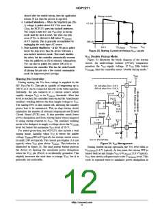
Figure 23. Startup Current at Various VCC Levels
V
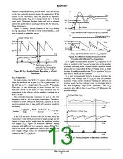
Double Hiccup Mode
CC
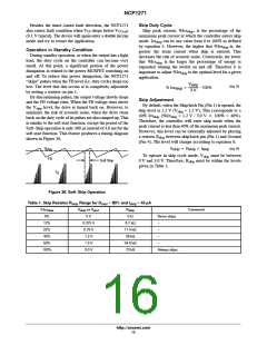
Figure 24 illustrates the block diagram of the startup
circuit. An undervoltage lockout (UVLO) comparator
monitors the V supply voltage. If V falls below
CC
CC
V
CC(off)
, then the controller enters “double hiccup mode.”
V
bulk
Biasing the Controller
HV
During startup, the Vcc bias voltage is supplied by the
HV Pin (Pin 8). This pin is capable of supporting up to
500 V, so it can be connected directly to the bulk capacitor.
Internally, the pin connects to a current source which
8
4.1 mA when Vcc > 0.6 V
200 uA when Vcc < 0.6 V
turn off
rapidly charges V to its V
threshold. After this
CC
CC(on)
level is reached, the controller turns on and the transformer
UVLO
+
auxiliary winding delivers the bias supply voltage to V
CC.
Q
S
R
−
The startup FET is then turned off, allowing the standby
power loss to be minimized. This in−chip startup circuit
minimizes the number of external components and Printed
Circuit Board (PCB) area. It also provides much lower
power dissipation and faster startup times when compared
12.6/
5.8 V
double
hiccup
B2
Counter
9.1 V
to using startup resistors to V . The auxiliary winding
CC
Vcc
needs to be designed to supply a voltage above the V
CC(off)
−
6
+
level but below the maximum V level of 20 V.
CC
For added protection, the NCP1271 also include a dual
&
20V
startup mode. Initially, when V is below the inhibit
CC
voltage V
(600 mV typical), the startup current source
inhibit
turn on internal bias
is small (200 uA typical). The current goes higher (4.1 mA
typical) when V goes above V . This behavior is
Figure 24. VCC Management
CC
inhibit
illustrated in Figure 23. The dual startup feature protects
the device by limiting the maximum power dissipation
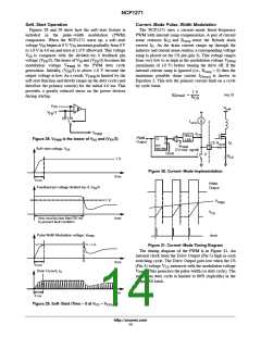
During double hiccup operation, the Vcc level falls to
(5.8 V typical). At this point, the startup FET is
V
CC(latch)
when the V pin (Pin 6) is accidentally grounded. This
turned back on and charges V to V
(12.6 V typical).
level. This
CC
CC
CC(on)
slightly increases the total time to charge V , but it is
V
CC
then slowly collapses back to the V
CC
CC(latch)
generally not noticeable.
cycle is repeated twice to minimize power dissipation in
http://onsemi.com
11

 ETC [ ETC ]