NCP1271
Soft−Start Operation
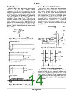
Current−Mode Pulse−Width Modulation
The NCP1271 uses a current−mode fixed−frequency
PWM with internal ramp compensation. A pair of current
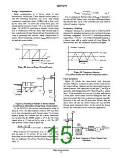
Figures 28 and 29 show how the soft−start feature is
included in the pulse−width modulation (PWM)
comparator. When the NCP1271 starts up, a soft−start
sense resistors R and R
sense the flyback drain
CS
ramp
voltage V begins at 0 V. V increasesgradually from 0 V
current I . As the drain current ramps up through the
SS
SS
D
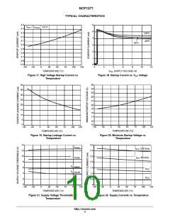
to 1.0 V in 4.0 ms and stays at 1.0 V afterward. This voltage
inductor and current sense resistor, a corresponding voltage
ramp is placed on the CS pin (pin 3). This voltage ranges
V
SS
is compared with the divided−by−3 feedback pin
voltage (V /3). The lesser of V and (V /3) becomes the
from very low to as high as the modulation voltage V
FB
SS
FB
PWM
modulation voltage V
in the PWM duty cycle
(maximum of 1.0 V) before turning the drive off. If the
PWM
generation. Initially, (V /3) is above 1.0 V because the
internal current ramp is ignored (i.e., R
≈ 0) then the
is shown in
FB
ramp
output voltage is low. As a result, V
is limited by the
maximum possible drain current I
PWM
D(max)
soft start function and slowly ramps up the duty cycle (and
therefore the primary current) for the initial 4.0 ms. This
provides a greatly reduced stress on the power devices
during startup.
Equation 2. This sets the primary current limit on a cycle
by cycle basis.
1 V
(eq. 2)
I
+
D(max)
R
CS
V
SS
/ 3
−
+
V
bulk
V
FB
0
1
I
ramp
V
V
PWM
CS
180ns
LEB
+
PWM
Output
−
Q
R
S
Figure 28. VPWM is the lesser of VSS and (VFB/3)
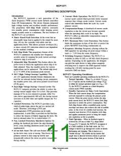
I
CS
R
D
ramp
80%
max duty
V
PWM
3
Soft−start voltage, V
SS
(1V max. signal)
1
Clock
0
R
CS
1 V
Figure 30. Current−Mode Implementation
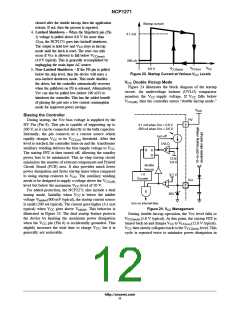
time
4 ms
PWM
Output
Feedback pin voltage divided−by−3, V /3
FB
1 V
V
PWM
V
CS
time must be less than130 ms
to prevent fault condition
time
Pulse Width Modulation voltage, V
clock
PWM
1 V
Figure 31. Current−Mode Timing Diagram
The timing diagram of the PWM is in Figure 31. An
internal clock turns the Drive Output (Pin 5) high in each
switching cycle. The Drive Output goes low when the CS
time
time
4 ms
Drain Current, I
(Pin 3) voltage V intersects with the modulation voltage
CS
V . This generates the pulse width (or duty cycle). The
PWM
D
maximum duty cycle is limited to 80% (typically) in the
output RS latch.
4 ms
Figure 29. Soft−Start (Time = 0 at VCC = VCC(on)
)
http://onsemi.com
13

 ETC [ ETC ]