NCP1271
V
time of 30 ns and 20 ns with a 1.0 nF load. This allows the
FB
NCP1271 to drive a high−current power MOSFET directly
for medium−high power application.
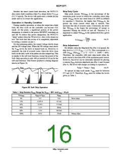
Fault operation when staying
in this region longer than 130 ms
3 V
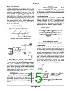
Noise Decoupling Capacitors
There are three pins in the NCP1271 that may need
external decoupling capacitors.
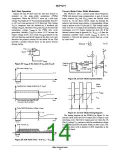
PWM operation
V
skip
0 V
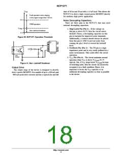
1. Skip/Latch Pin (Pin 1) – If the voltage on
this pin is above 8.0 V, then the circuit enters
latchoff. Hence, a decoupling capacitor on this
pin is essential for improved noise immunity.
Additionally, a resistor should always be placed
from this pin to GND to prevent noise from
causing the pin 1 level to exceed the latchoff
level.
Non−latched shutdown
Figure 40. NCP1271 Operation Threshold
1
2
8
3
6
5
2. Feedback Pin (Pin 2) – The FB pin is a high
impedance point and is very easily polluted in a
noisy environment. This could effect the circuit
operation.
OFF
4
NCP1271
opto
coupler
3. V Pin (Pin 6) – The circuit maintains normal
CC
operation when V is above V
(9.1 V
CC
CC(off)
typical). But, if V drops below V
of switching noise, then the circuit can incorrectly
recognize it as a fault condition. Hence, it is
because
CC
CC(off)
Figure 41. Non−Latchoff Shutdown
Output Drive
important to locate the V capacitor or an
CC
The output stage of the device is designed to directly
drive a power MOSFET. It is capable of up to +500 mA and
−800 mA peak drive currents and has a typical rise and fall
additional decoupling capacitor as close as possible
to the device.
http://onsemi.com
17

 ETC [ ETC ]