NCP1271
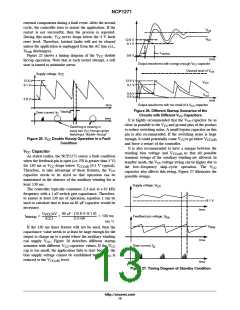
Recover from Standby
to be opened. The skip level V
the default 1.2 V.
is restored to
skip
In the event that a large load is encountered during skip
cycle operation, the circuit automatically disables the
normal Soft−Skip procedure and delivers maximum power
to the load (Figure 37). This feature, the Transient Load
Detector (TLD), is initiated anytime a skip event is exited
and the FB pin is greater than 2.85 V, as would be the case
for a sudden increase in output load.
3. When the voltage is between about 3.0 V and
, the V level is above the normal
V
skip−reset
skip
operating range of the feedback pin. Therefore,
the output does not switch.
4. When the voltage is between 0 V and 3.0 V, the
V
skip
is within the operating range of the
feedback pin. Then the voltage on this pin sets
the skip level as explained earlier.
output voltage
300 ms max
V
pin1
10 V (max limit)
Output is latched off here.
8V (V
load current
V
)
TLD
latch
Maximum current available
Pin 1 considered to be opened.
is reset to default level 1.2 V.
when TLD level is hit
V
skip
V
skip
V
FB
5.7 V (V
)
skip−reset
Output always low (skipped) here.
3.0 V (always skip)
I
D
Figure 37. Transient Response from Standby
Adjustable V
range.
skip
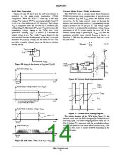
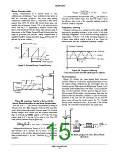
External Latchoff Shutdown
When the Skip/Latch input (Pin 1) is pulled higher than
0 V (no skip)
V
V
(8.0 V typical), the drive output is latched off until
latch
drops below V
(4.0 V
). If Vbulk stays
typical
CC
CC(reset)
Figure 39. NCP1271 Pin 1 Operating Regions
The external latch feature allows the circuit designers to
implement different kinds of latching protection. The
NCP1271 applications note (AND8242/D) details several
simple circuits to implement overtemperature protection
(OTP) and overvoltage protection (OVP).
above approximately 30 Vdc, then the HV FET ensure that
remains above V (5.8 V ). Therefore, the
V
CC
CC(latch)
typical
controller is reset by unplugging the power supply from the
wall and allowing V to discharge. Figure 38 illustrates
the timing diagram of V in the latchoff condition.
bulk
CC
In order to prevent unexpected latchoff due to noise,
it is very important to put a noise decoupling capacitor
near Pin 1 to increase the noise immunity. It is also
recommended to always have a resistor from pin 1 to GND.
This further reduces the risk of premature latchoff. Also
note that if the additional latch−off circuitry has leakage,
it will modify the skip adjust setup.
Startup current source is
Startup current source is
off when V is 12.6 V
charging the V capacitor
CC
CC
12.6 V
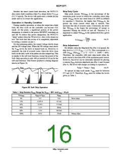
External Non−Latched Shutdown
Figure 40 illustrates the Feedback (pin 2) operation. An
external non−latched shutdown can be easily implemented
by simply pulling FB below the skip level. This is an
inherent feature from the standby skip operation. Hence, it
allows the designer to implement additional non−latched
shutdown protection.
5.8 V
Startup current source turns
on when V reaches 5.8 V
CC
CC
Figure 38. Latchoff VCC Timing Diagram
Figure 39 defines the different voltage regions of the
Skip/latch Pin (Pin 1) operation.
The device can also be shutdown by pulling the V pin
CC
to GND (<190 mV). In addition to shutting off the output,
this method also places the part into a low current
consumption state.
1. When the voltage is above V
(7.1 V min,
latch
8.7 V max), the circuit is in latchoff and all drive
pulses are disabled until V cycles below 4.0 V
CC
(typical).
2. When the voltage is between V
(5.0 V
skip−reset
min, 6.5 V max) and V
, the pin is considered
latch
http://onsemi.com
16

 ETC [ ETC ]