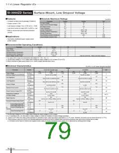
1-1-4 Linear Regulator ICs
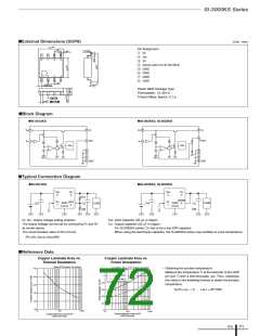
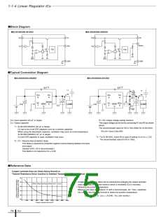
■Block Diagram
●SI-3010KD/SI-3012KD
●SI-3033KD/SI-3050KD
V
IN
2
1
4
5
VO
V
IN
2
4
5
Vo
Sense
ADJ
V
C
V
C
1
TSD
TSD
-
-
+
+
REF
REF
3
3
GND
GND
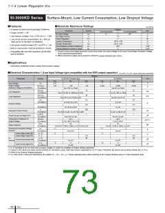
■Typical Connection Diagram
●SI-3033KD/SI-3050KD
●SI-3010KD/SI-3012KD
D1*2
D1*2
*1
*3
R3
*1
V
IN
VO
V
IN
VO
2
4
2
4
R1
+
+
+
+
sense
5
V
1
C
V
1
C
ADJ
5
GND
3
GND
3
Load
Load
C
IN
C
IN
CO
C
O
R2
CIN: Input capacitor (22 µF or larger)
R1, R2: Output voltage setting resistors
CO: Output capacitor
The output voltage can be set by connecting R1 and R2 as shown
above.
*1: SI-3012KD/3033KD (22 µF or larger)
The recommended value for R2 is 10Ω (24kΩ for SI-3012KD).
Co has to be a low ESR capacitor such as a ceramic capacitor.
When using the electrolytic capacitor, oscillation may occur at a low temperature.
SI-3010KD/3050KD/ (47 µF or larger)
R1=(VO–VADJ)÷(VADJ/R2)
If a low ESR capacitor is used, oscillation may occur.
*3: For SI-3010KD, insert R3 in case of setting VO to VO ≤ 1.5V.
The recommended value for R3 is 10kΩ.
*2: D1: Reverse bias protection diode
This diode is required for protection against reverse biasing between the input
and output.
(Sanken SJPL-H2 is recommended.)
This diode is not required at VO ≤ 3.3V.
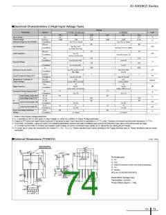
■Reference Data
Copper Laminate Area (on Glass-Epoxy Board) vs.
Thermal Resistance (from Junction to Ambient Temperature) (Typical Value)
55
50
45
40
35
30
• A higher heat radiation effect can be achieved by enlarging the copper laminate
area connected to the inner frame to which a monolithic ICs is mounted.
• Obtaining the junction temperature
When Using Glass-Epoxy Board of 40 × 40 mm
θ
Measure the case temperature TC with a thermocouple, etc. Then, substitute
this value in the following formula to obtain the junction temperature.
Tj=PD × θj–C + TC ( θj–C = 3°C/W) PD= (VIN–VO)•IOUT
0
200
400
600
800
1000 1200 1400 1600 1800
Copper Laminate Area (mm2)
ICs
74

 ETC [ ETC ]