SI-3000KD Series
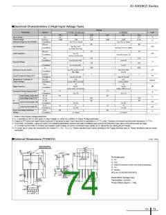
■Electrical Characteristics 2 (High Input Voltage Type)
Ratings
Parameter
Symbol
SI-3010KD (Variable type)
typ.
SI-3050KD
typ.
Unit
min.
2.4*1
0.98
max.
27*5
min.
*1
max.
15*5
Input Voltage
VIN
V
V
Output Voltage
VO
(VADJ
)
1.00
1.02
4.90
5.00
5.10
(Reference Voltage VADJ for SI-3010KD)
Conditions
V
IN=7V, I
O
=10mA
VIN=7V, IO=10mA
∆VOLINE
30
75
30
75
mV
mV
Line Regulation
Load Regulation
V
IN=6 to 11V,
Conditions
∆VOLOAD
VIN=6 to 11V, IO=10mA
I
O
=10mA (V =5V)
O
V
IN=7V,
Conditions
V
IN=7V, IO=0 to 1A
IO
=0 to 1A (VO=5V)
V
DIF
0.3
0.6
600
0.3
0.6
600
Conditions
I
O
=0.5A (V
O
=5V)
I
O
=0.5A
V
Dropout Voltage
Conditions
I
O
=1A (V
O
=5V)
IO
=1A
I
q
µ
A
A
Quiescent Circuit Current
V
IN=7V, I
O
=0A, V
C
=2V
V
IN=7V, I
O=0A,
Conditions
R2=10kΩ
V
C=2V
I
q
(OFF)
1
1
µ
Circuit Current at Output OFF
Conditions
V
IN=7V, V
C
=0V
V
IN=7V, V
0.5
C=0V
Temperature Coefficient of
Output Voltage
∆VO/∆Ta
0.5
mV/°C
Conditions
T
j
=0 to 100°C (V
O
=5V)
Tj=0 to 100°C
RREJ
75
75
dB
Ripple Rejection
V
IN=7V,
V
IN=7V,
Conditions
f=100 to 120Hz, I =0.1A (V
O
O=5V)
f=100 to 120Hz, IO=0.1A
*2
I
S1
1.1
2.0
1.1
2.0
Overcurrent Protection Starting Current
*4
A
V
Conditions
, IH
V
IN=7V
VIN=7V
*3
Control Voltage (Output ON)
VC
*3
Control Voltage (Output OFF)
V
C
, IL
0.8
40
0.8
40
VC
I
C, IH
µ
A
A
Control Current (Output ON)
Control Current (Output OFF)
Terminal
Conditions
, IL
Conditions
VC
=2V
V
V
C
=2V
0
I
C
–5
33
0
–5
26
µ
VC
=0V
C=0V
Input Overvoltage Shutdown
Voltage
VOVP
V
Conditions
I
O
=10mA
IO=10mA
*1: Refer to the Dropout Voltage parameter.
*2: Is1 is specified at the 5% drop point of output voltage VO under the condition of Output Voltage parameter.
*3: Output is OFF when the output control terminal (VC terminal) is open. Each input level is equivalent to LS-TTL level. Therefore, the device can be driven directly by LS-TTLs.
*4: SI-3010KD, SI-3050KD, cannot be used in the following applications because the built-in foldback-type overcurrent protection may cause errors during start-up stage.
(1) Constant current load (2) Positive and negative power supply (3) Series-connected power supply (4) VO adjustment by raising ground voltage
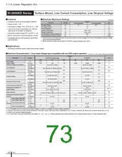
*5: VIN (max) and IO (max) are restricted by the relation PD = (VIN - VO) ✕ IO. Please calculate these values referring to the Copper laminate area vs. Power dissipation data as shown
hereinafter.
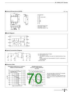
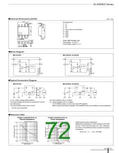
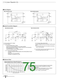
■External Dimensions (TO263-5)
(unit : mm)
Case temperature
measurement point
0.2
10.0
(8.0)
(4.4)
(15°)
0.2
4.5
+0.10
–0.05
1.3
3-R0.3
Pin Assignment
q VC
0.2
(2×R0.45)
(3°)
φ1.5 Dp:
w VIN
e GND (Common to the rear side of product)
0.15
0.10
(3°)
r VO
(3°)
0.2
2.4
(R0.3)
t Sense
(ADJ for SI-3010KD/3012KD)
0.10
0.25
0.88
(1.7
(R0.3)
0 to 6°
(0.5)
Plastic Mold Package Type
Flammability: UL94V-0
0.1
0.1
0.8
(1.7
0.8
(1.7
0.25
0.25
0.25
)
(1.7
)
)
)
1
2
3
4
5
Product Mass: Approx. 1.48g
0.2
9.9
(3°)
(3°)
2-R0.3
0.02
10.0
ICs
73

 ETC [ ETC ]