SI-3000LLSL Series
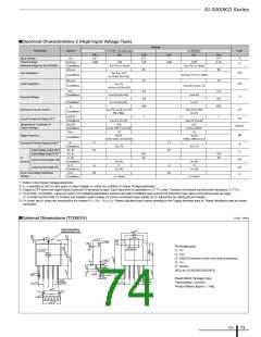
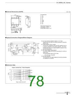
■External Dimensions (SOP8)
(unit : mm)
Pin Assignment
q VO
5.1±0.4
1.27
+0.1
0.4±0.1
0.15
–0.05
w ADJ
e VB
8
1
7
6
3
5
4
r VC
t GND
y GND
u VIN
i VIN
2
Plastic Mold Package Type
Flammability: UL94V-0
1.27
0.995max.
Product Mass: Approx. 0.1g
0.10
0.4±0.1
0.12 M
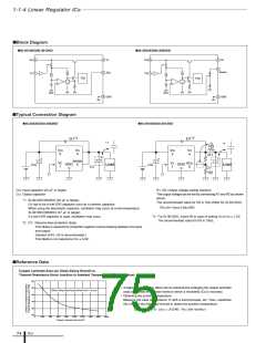
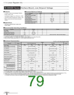
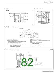
■Typical Connection Diagram/Block Diagram
CIN, CB: Input and bias capacitors (Approx. 0.1 to 10µF)
Required when the input line contains inductance or when the
wiring is long.
VOUT
1
VIN
7
+
CO: Output capacitor (47µF or larger)
CSS
R1
8
R1
SI-3010LLSL is designed to use a low ESR capacitor (such as
a ceramic capacitor) for the output capacitor. The recom-
mended ESR value for an output capacitor is 500mΩ or less
(at room temperature).
CIN
VB
+
OCP(2)
Drive
OCP
REF
3
ADJ
2
CO
+
TSD
-
+
R2
R1, R2: Output voltage setting resistors
AMP1
-
ON/OFF
6
5
CB
VC
The output voltage can be set by connecting R1 and R2 as
shown at left.
4
-
+
Open:OFF
Low: OFF
High: ON
GND
The recommended value for R2 is 10kΩ.
R1= (VO–VADJ) / (VADJ/R2)
CSS:Soft start capacitor
The rising time of the output voltage can be set by connecting
CSS between VOUT and ADJ.
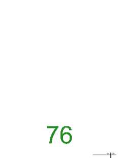
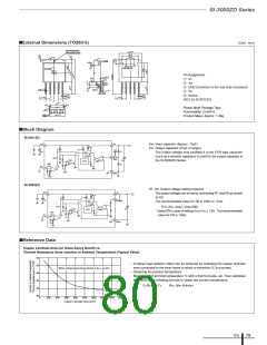
■Reference Data
Copper Laminate Area - Power Dissipation
1.2
1
Ta=25°C
Ta=50°C
Ta=80°C
0.8
0.6
0.4
0.2
0
10
100
1000
Copper Laminate Area (mm2)
ICs
77

 ETC [ ETC ]