SI-3000KS Series
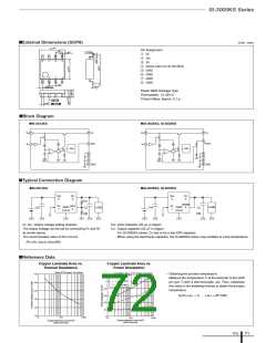
■External Dimensions (SOP8)
(Unit : mm)
5.1±0.4
Pin Assignment
1.27
+0.1
0.4±0.1
0.15
–0.05
q VC
w VIN
8
1
7
6
3
5
4
e VO
r Sence (ADJ for SI-3012KS)
t GND
y GND
u GND
i GND
2
1.27
0.995max.
Plastic Mold Package Type
Flammability: UL 94V-0
Product Mass: Approx. 0.1 g
0.10
0.4±0.1
0.12 M
■Block Diagram
●SI-3012KS
●SI-3025KS, SI-3033KS
V
IN
2
1
3
V
O
V
IN
2
1
3
4
VO
Sense
4
ADJ
V
C
VC
TSD
TSD
-
-
+
+
8
7
6
5
8
7
6
5
REF
REF
GND
GND
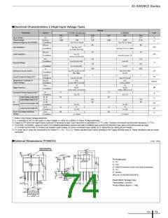
■Typical Connection Diagram
●SI-3012KS
●SI-3025KS, SI-3033KS
VIN
2
VO
3
V
IN
VO
3
2
R1
CO
R2
sense
4
VC
1
ADJ
4
VC
1
GND
5 to 8
GND
5 to 8
Load
Load
CIN
C
IN
CO
R2
R1, R2: Output voltage setting resistors
CIN: Input capacitor (22 µF or larger)
CO: Output capacitor (22 µF or larger)
The output voltage can be set by connecting R1 and R2
as shown above.
For SI-3000KS series, Co has to be a low ESR capacitor.
The recommended value of R2 is 24 kΩ .
When using the electrolytic capacitor, the SI-3000KS series may oscillate at a low temperature.
R1=(VO–VADJ)÷(VADJ/R2)
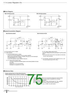
■Reference Data
Copper Laminate Area vs.
Thermal Resistance
Copper Laminate Area vs.
Power Dissipation
Area of PC board : 40×40mm
Tj=100°C Area of PC board : 40×40mm
140
• Obtaining the junction temperature
1.2
1
Ta=25°C
Measure the temperature TL at the lead part of the GND
Ta=50°C
pin (pin 7) with a thermocouple, etc. Then, substitute
120
Ta=80°C
this value in the following formula to obtain the junction
0.8
temperature.
θ
100
0.6
0.4
Tj=PD × θj–L + TL
( θj–L = 22°C/W)
80
60
40
0.2
0
10
100
1000
10
100
1000
Copper laminate area (mm2)
(GND terminal)
Copper laminate area (mm2)
(GND terminal)
ICs
71

 ETC [ ETC ]