1-1-4 Linear Regulator ICs
SI-3000ZD Series Surface-Mount, Low Dropout Voltage
■Features
■Absolute Maximum Ratings
(Ta=25°C)
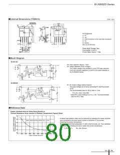
• Compact surface-mount package (TO263-5)
Parameter
Symbol
Ratings
Unit
V
*1
DC Input Voltage
VIN
10
• Output current: 3.0A
Output Control Terminal Voltage
DC Output Current
VC
6
V
• Low dropout voltage: VDIF ≤ 0.6V (at IO = 3.0A)
*1
IO
3.0
3
A
*3
•
Low circuit current at output OFF: Iq (OFF) ≤ 1µA
Power Dissipation
PD
W
Junction Temperature
Tj
–30 to +125
–30 to +85
–40 to +125
33.3
°C
• Built-in overcurrent and thermal protection
circuits
Operating Ambient Temperature
Storage Temperature
Top
Tstg
θj-a
θj-c
°C
°C
Thermal Resistance (Junction to Ambient Air)
Thermal Resistance (Junction to Case)
°C/W
°C/W
■Applications
3
• Secondary stabilized power supply (local
power supply)
■Recommended Operating Conditions
Parameter
Symbol
Ratings
*2 to 6*1
Unit
Remarks
Input Voltage
VIN
V
A
Output Current
IO
0 to 3
Operating Ambient Temperature
Operating Junction Temperature
Output Voltage Variable Range
Top (a)
Top (j)
VOADJ
–20 to +85
–20 to +100
1.2 to 5
°C
°C
V
Only for SI-3011ZD. Refer to the block diagram.
*1: VIN (max) and IO (max) are restricted by the relation PD = (VIN - VO) × IO.
*2: Set the input voltage to 2.4V or higher when setting the output voltage to 2.0V or lower (SI-3011ZD).
*3: When mounted on glass-epoxy board of 40 × 40mm (copper laminate area 100%).
■Electrical Characteristics
(Ta=25°C, VC=2V, unless otherwise specified)
Ratings
Parameter
Symbol
SI-3011ZD (Variable type)
SI-3033ZD
typ.
Unit
min.
typ.
1.100
max.
min.
max.
Output Voltage
VO (VADJ)
Conditions
∆VOLINE
Conditions
∆VOLOAD
Conditions
VDIF
1.078
1.122
3.234
3.300
3.366
V
mV
mV
V
(Reference Voltage VADJ for SI-3011ZD)
Line Regulation
VIN=VO+1V, IO=10mA
VIN=5V, IO=10mA
10
40
0.6
1.5
1
10
40
0.6
1.5
1
V
IN=3.3 to 5V, I
O
=10mA (V
O
=2.5V)
VIN=4.5 to 5.5V, IO=10mA
VIN=5V, IO=0 to 3A
Load Regulation
VIN=3.3V, IO=0 to 3A (VO=2.5V)
Dropout Voltage
Conditions
Iq
IO=3A (VO=2.5V)
IO=3A
1
1
Quiescent Circuit Current
Circuit Current at Output OFF
mA
µA
mV/°C
dB
Conditions
Iq (OFF)
Conditions
∆VO/∆Ta
Conditions
RREJ
VIN=VO+1V, IO=0A, VC=2V
VIN=5V, IO=0A, VC=2V
VIN=VO+1V, VC=0V
VIN=5V, VC=0V
Temperature Coefficient
of Output Voltage
±0.3
±0.3
Tj=0 to 100°C
Tj=0 to 100°C
60
60
Ripple Rejection
Conditions
IS1
VIN=VO+1V, f=100 to 120HZ, IO=0.1A
VIN=5V, f=100 to 120HZ, IO=0.1A
*2
3.2
2
3.2
2
Overcurrent Protection Starting Current
A
*4
Conditions
VC, IH
VIN=VO+1V
VIN=5V
*3
Control Voltage (Output ON)
V
*3
Control Voltage (Output OFF)
VC, IL
0.8
0.8
V
C
Control Current(Output ON)
IC, IH
100
100
µA
µA
Terminal
Conditions
IC, IL
VC=2.7V
0
VC=2.7V
0
Control Current(Output OFF)
–5
–5
Conditions
VC=0V
VC=0V
*1: Set the input voltage to 2.4V or higher when setting the output voltage to 2.0V or lower.
*2: IS1 is specified at the –5% drop point of output voltage VO under the condition of Output Voltage parameter.
*3: Output is OFF when the output control terminal (VC terminal) is open. Each input level is equivalent to LS-TTL level. Therefore, the device can be driven directly by LS-TTLs.
*4: These products cannot be used for the following applications because the built-in foldback-type overcurrent protection may cause errors during start-up stage.
(1) Constant current load (2) Positive and negative power supply (3) Series-connected power supply (4) VO adjustment by raising ground voltage
ICs
78

 ETC [ ETC ]