1-1-4 Linear Regulator ICs
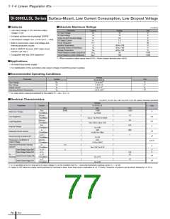
SI-3000KD Series Surface-Mount, Low Current Consumption, Low Dropout Voltage
■Features
■Absolute Maximum Ratings
(Ta=25°C)
• Compact surface-mount package (TO263-5)
Ratings
Parameter
Symbol
Unit
3033KD
SI-3012KD/
SI-3010KD/3050KD
35*1
• Output current: 1.0A
DC Input Voltage
VIN
IO
17
V
A
• Low dropout voltage: VDIF ≤ 0.6V (at IO = 1.0A)
DC Output Current
1.0
*2
Power Dissipation
PD
3
–30 to +125
–30 to +125
33.3
W
• Low circuit current consumption: Iq ≤ 350 µA
(600 µA for SI-3010KD, SI-3050KD)
Junction Temperature
Tj
°C
Storage Temperature
Tstg
θj-a
θj-c
°C
•
Low circuit current at output OFF: Iq (OFF) ≤ 1 µA
Thermal Resistance (Junction to Ambient Air)
Thermal Resistance (Junction to Case)
°C/W
°C/W
• Built-in overcurrent, thermal protection circuits
3
*1: A built-in input-overvoltage-protection circuit shuts down the output voltage at the Input Overvoltage Shutdown Voltage
of the electrical characteristics.
*2: When mounted on glass-epoxy board of 1600mm2 (copper laminate area 100%).
•
Compatible with low ESR capacitors (SI-3012KD
and SI-3033KD)
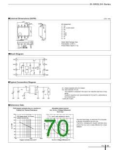
■Applications
• Secondary stabilized power supply (local power supply)
■Electrical Characteristics 1 (Low Input Voltage type compatible with low ESR output capacitor)
(Ta=25°C, VC=2V, unless otherwise specified)
Ratings
Parameter
Symbol
SI-3012KD (Variable type)
typ.
SI-3033KD
Unit
min.
2.4*3
1.24
max.
*4
min.
*3
typ.
max.
*4
Input Voltage
VIN
V
V
Output Voltage
(Reference Voltage for SI-3012KD)
VO (VADJ)
Conditions
∆VOLINE
1.28
1.32
15
3.234
3.300
3.366
15
VIN=3.3V, IO=10mA
VIN=5V, IO=10mA
mV
mV
Line Regulation
Load Regulation
Conditions
∆VOLOAD
Conditions
VDIF
VIN=3.3 to 8V, IO=10mA (VO=2.5V)
VIN=5 to 10V, IO=10mA
VIN=5V, IO=0 to 1A
IO=0.5A
40
50
V
IN=3.3V, IO=0 to 1A (VO=2.5V)
0.4
0.6
350
1
0.4
0.6
350
1
Conditions
IO=0.5A (VO=2.5V)
IO=1A (VO=2.5V)
V
Dropout Voltage
Conditions
Iq
IO=1A
µA
µA
Quiescent Circuit Current
Conditions
Iq (OFF)
Conditions
∆VO/∆Ta
Conditions
RREJ
VIN=3.3V, IO=0A, VC=2V, R2=2.4kΩ
VIN=5V, IO=0A,VC=2V
Circuit Current at Output OFF
VIN=3.3V, VC=0V
VIN=5V, VC=0V
Temperature Coefficient of
Output Voltage
±0.3
±0.3
Tj=0 to 100°C
mV/°C
dB
Tj=0 to 100°C (VO=2.5V)
55
55
Ripple Rejection
Conditions
IS1
VIN=3.3V, f=100 to 120HZ, IO=0.1A (VO=2.5V)
1.1
VIN=5V, f=100 to 120HZ, IO=0.1A
Overcurrent Protection Starting
1.1
2
A
*1
Current
Conditions
VC, IH
VIN=3.3V
VIN=5V
*2
Control Voltage (Output ON)
2
V
Control Voltage (Output OFF)
Control Current (Output ON)
VC, IL
0.8
40
0.8
40
VC
IC, IH
µA
Terminal
Conditions
IC, IL
VC=2V
0
VC=2V
0
–5
–5
µA
Control Current (Output OFF)
Conditions
VC=0V
VC=0V
*1: IS1 is specified at the 5% drop point of output voltage VO under the condition of Output Voltage parameter.
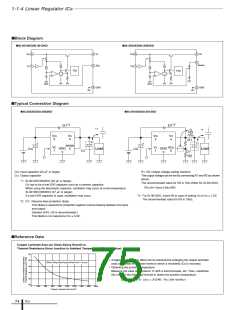
*2: Output is OFF when the output control terminal (VC terminal) is open. Each input level is equivalent to LS-TTL level. Therefore, the device can be driven directly by LS-TTLs.
*3: Refer to the Dropout Voltage parameter.
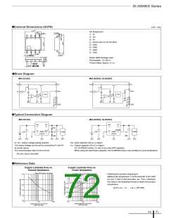
*4: VIN (max) and IO (max) are restricted by the relation PD = (VIN - VO) × IO. Please calculate these values referring to the Copper laminate area vs. Power dissipation data.
ICs
72

 ETC [ ETC ]