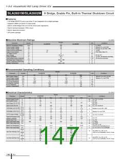
1-3-2 Household HID Lamp Driver ICs
SLA2601M/SLA2602M H Bridge, Enable Pin, Built-in Thermal Shutdown Circuit
■Features
• Full-bridge MOSFETs and a pre-drive IC are integrated into a single package
• Supports CMOS (3.3 and 5 V) input levels
• Built-in undervoltage lock out (UVLO) circuit (auto regression)
• Built-in thermal shutdown (TSD) circuit
• Built-in dead time function
• SIP power package
(T a=25 )
a
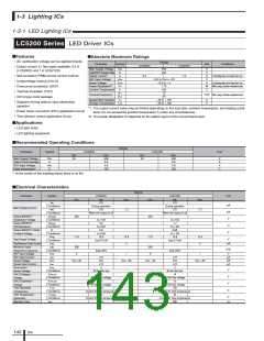
■Absolute Maximum Ratings
(T =25℃)
Ratings
Parameter
Symbol
Unit
Conditions
SLA2601M
SLA2602M
MOSFET Breakdown Voltage
Control Supply Voltage
Control Supply Voltage
Output Current (continuous)
Output Current (pulse)
FO Output Current
Input Voltage
Power Dissipation
Thermal Resistance (Junction to Ambient Air)
Operating Case Temperature
Junction Temperature (Power part)
Storage Temperature
VDSS
Vcc
VBS
Io
250
20
20
V
V
V
A
A
ID=100uA
Between VCC and COM
Between VB and VM1, VM2
Tc=25℃
14
21
7
10.5
IOP
IFO
VIN
PD
PW≤100µs, duty=1%
8
mA
V
–0.5 to +7
41.6
3.0
–20 to +100
150
–40 to +150
EN, IN, FO
TC=25℃, all elements operating
All elements operating
W
℃/W
℃
℃
℃
θj-c
TOP
Tj
Tstg
■Recommended Operating Conditions
Ratings
Parameter
Symbol
SLA2601M
SLA2602M
Unit
Conditions
min.
-
13.5
10
0.68
0.001
-
max.
min.
-
13.5
10
0.68
0.001
-
max.
200
17.5
-
Main Supply Voltage
Control Supply Voltage
Boot Strap Capacitor Capacity
FO Pull-up Resistance
FO Capacitor Capacity
IN Pin Frequency
VBB
Vcc
Cboot
RFO
CFO
FIN
200
17.5
-
V
V
Between VBB and LS/COM
Between VCC and COM
uF
kΩ
uF
kHz
℃
10
10
0.01
150
125
0.01
150
125
Junction Temperature
Tj
-
-
(Ta=25℃)
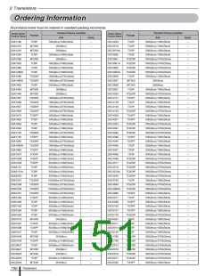
■Electrical Characteristics
Ratings
Parameter
Symbol
SLA2601M
typ.
2
135
2
1.5
230
-
SLA2602M
typ.
2
135
2
1.5
230
-
Unit
Conditions
O=OPEN
min.
-
-
-
1
max.
-
-
2.5
-
500
11
11.5
12
12.5
1
min.
-
-
-
1
max.
-
-
2.5
-
500
11
11.5
12
12.5
1
Control Supply Current
Boot Supply Current
I
cc
mA
uA
V
V
V
V
V
cc=15V, F
IB
B=15V
V
IH
IL
IH
UVHL
UVHH
UVLL
UVLH
cc=15V
cc=15V
Input Voltage (EN, IN, FO)
Input Current (EN, IN)
Undervoltage Lock Out (VB)
V
V
I
V
-
9
-
9
uA
cc=15V, EN,IN=5V
and VM1, VM2
Between VCC and COM
V
V
Between VB
V
9.5
10
10.5
0
3.6
135
105
-
-
-
-
-
9.5
10
10.5
0
3.6
135
105
-
-
-
-
-
V
V
Undervoltage Lock Out (VCC
FO Pin Output Voltage
)
V
FO(L)
V
V
cc=15V, FO=OPEN
VFO(H)
-
5
-
5
Thermal Protection and
Release Threshold
Internal Dead Time
T
DH
DL
dead
DSS
DSS
150
120
430
-
165
135
-
-
100
150
120
430
-
165
135
-
-
100
℃
V
cc=15V
cc=15V
T
T
V
I
ns
V
uA
V
MOSFET Output Breakdown Voltage
MOSFET Output Leakage Current
250
-
250
-
I
V
V
D
=100uA
DS=250V
CC=15V, I
-
-
D=7A
MOSFET DC ON Resistance RDS(on)
-
0.11
0.14
-
0.14
0.185
Ω
(3.5A for the SLA2602M),EN=5V
MOSFET Diode Forward Voltage
V
td(on)
tr
td(off)
tf
td(on)
tr
SD
-
-
-
-
-
-
-
-
-
1
1.5
-
-
-
-
-
-
-
-
-
-
-
-
-
-
-
-
-
1
1260
40
850
15
1240
40
830
25
1.5
-
-
-
-
-
-
-
-
V
ISD=7A (3.5A for the SLA2602M)
1290
100
900
30
1270
80
ns
ns
VBB=200V, VCC=15V, I
D=7A
High Side Switching Time
(3.5A for the SLA2602M), EN=5V, R load
VBB=200V, VCC=15V, I
D=7A
Low Side Switching Time
td(off)
tf
880
30
(3.5A for the SLA2602M), EN=5V, R load
ICs
146

 ETC [ ETC ]