1-3 Lighting ICs
1-3-1 LED Lighting ICs
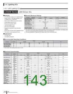
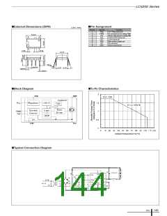
LC5200 Series
■Features
LED Driver ICs
■Absolute Maximum Ratings
• AC rectification voltage can be applied directly
Ratings
Parameter
Symbol
Unit
Conditions
LC5205D
LC5210D
1.0
• Output current IO: Two types available: 0.5 A
(LC5205D) and 1 A (LC5210D)
Main Supply Voltage
Output MOSFET Breakdown Voltage
Output current*1
VBB
Vo
450
450
V
V
A
V
V
• Self-excitation PWM current control method
• Undervoltage lockout (UVLO)
• Overcurrent protection (OCP)
• Thermal shutdown (TSD)
Io
0.5
Excluding when tw is less than 1µs
REF Input Voltage
Sense Voltage
Power Dissipation*2
VRef
VSen
PD
–0.3 to VREG + 0.3
–0.3 to + 4
1.73
Excluding when tw is less than 1µs
When using a Sanken evaluation board
W
℃
Junction Temperature
Tj
150
72
60
θj-a
θc-a
Ta
Thermal Resistance
℃/W When using a Sanken evaluation board
• DIP-8 type mold package
Operating Ambient Temperature
–40 to + 105
–40 to + 150
℃
℃
• Supports driving without input electrolytic
capacitor
Storage Temperature Tstg
*1: The output current value may be limited depending on the duty ratio, ambient temperature, and heating condi-
tions. Do not exceed the junction temperature Tj under any circumstances.
• Power factor correction (PFC) application circuit
• Triac dimmer control application circuit
*2: The power dissipation PD depends on the pattern layout of the circuit board used.
■Applications
• LED light bulbs
• LED lighting equipment
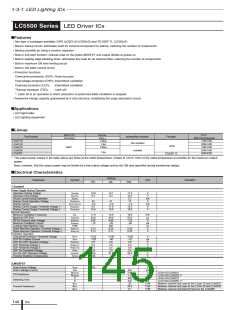
■Recommended Operating Conditions
Ratings
Parameter
Symbol
LC5205D
LC5210D
Unit
min.
25
max.
400
0.4
0.8
105
min.
25
max.
400
0.8
0.8
105
Main Supply Voltage
Output Current (Average)
REF Input Voltage
Case temperature*
VBB
Io
V
A
V
VRef
Tc
℃
*: At the center of the marking (when there is no fin)
■Electrical Characteristics
Ratings
Parameter
Symbol
LC5205D
LC5210D
Unit
min.
450
typ.
2.0
max.
min.
typ.
2.0
max.
1.2
I
BB
mA
mA
V
Conditions
During operation
0.8
When the output is off
During operation
0.8
When the output is off
Main Supply Current
IBBs
1.2
Conditions
Output MOSFET
Breakdown Voltage
Output MOSFET
ON Resistance
Output MOSFET Diode
Forward Voltage
V
DS(BR)
450
Conditions
I
I
I
D
D
D
=1mA
3.5
=0.5A
0.8
=0.5A
I
I
I
D
=1mA
1.7
=1.0A
0.88
=1.0A
R
DS(on)
Ω
Conditions
V
Conditions
D
F
V
D
V
Reg
11.5
12.0
12.5
2
11.5
12.0
12.5
2
Reg Output Voltage
V
Conditions
I
Reg=0.1mA
I
Reg=0.1mA
Reg Maximum Output Current
Maximum Input
Response Frequency
REF Input Voltage
REF Input Current
Sense Voltage
Sense Input Current
Overcurrent
IReg
mA
fclk
Conditions
200
0
200
0
kHz
duty=50%
10
duty=50%
10
V
Ref
Ref
Sen
Sen
ocp
1
1
V
I
V
I
V
µA
mV
µA
V
Ref –30
V
Ref
V
Ref +30
V
Ref –30
V
Ref
V
Ref +30
10
3
10
3
V
V
Sense Voltage
UVLO Release
Voltage
Conditions
At the Sen pin
At the Sen pin
VUVLOon
14
14
Conditions
At the VBB voltage
At the VBB voltage
UVLO Operation
Voltage
V
UVLOoff
13
13
V
Conditions
At the VBB voltage
At the VBB voltage
TSD Operating
Temperature
T
TSD
150
150
℃
Conditions
Control IC chip temperature
Control IC chip temperature
TSD Temperature
Hysteresis
Blanking Time
T
TSDhys
55
Control IC chip temperature
400
55
Control IC chip temperature
400
℃
Conditions
t
BLK
ns
ICs
142

 ETC [ ETC ]