LC5500 Series
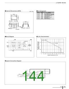
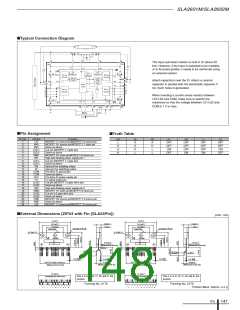
■Pin Assignment
LC5511D/LC5513D
LC5521D/LC5523D/LC5523F
Pin No.
Pin Symbol
Function
Pin No.
Symbol
S/GND
VCC
Function
MOSFET source/GND for control
Control circuit power input
1
2
3
4
5
6
8
LC5521D/LC5523D LC5523F
1
2
3
4
5
6
8
2
4
5
6
3
7
1
S/GND
VCC
OCP
FB
NF(NC)
OVP
D/ST
MOSFET source/GND for control
Control circuit power input
OCP
COMP
NF
Overcurrent protection/Quasi-Resonant signal input
Feedback phase compensation
-
Overcurrent protection/Quasi-Resonant signal input
Feedback signal input/overload protection signal input
-
Overvoltage protection signal input
MOSFET drain/startup current input
ISENSE
D/ST
Feedback current detection
MOSFET drain/startup current input
■Typical Connection Diagram
LC5511D/LC5513D
LC5521D/LC5523D/LC5523F
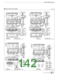
■External Dimensions (DIP8/TO220F-7L)
(Unit : mm)
DIP8
TO220F-7L
4.2 0.2
2.6 0.2
9.4 0.3
Gate burr
8
5
LC
(1.1)
a
b
2.6 0.1
(Measured
at the root)
1
4
1.52
+0.3
-0.05
+0.3
-0.05
1.0
7.6TYP
7-0.62 0.15
+0.2
–0.1
7-0.55
5×P1.17 0.15
+0.2
–0.1
0.45
=5.85 0.15
2
0.15
(Measured at the root)
10.1 0.2
2.54TYP
0~15° 0~15°
0.89TYP
0.5 0.1
1
2 3 4 5 6 7
ICs
145

 ETC [ ETC ]