1-3-1 LED Lighting ICs
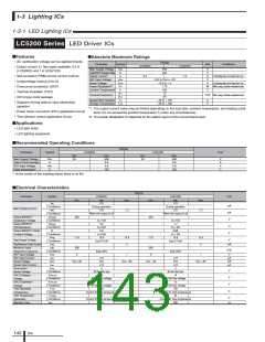
LC5500 Series LED Driver ICs
■Features
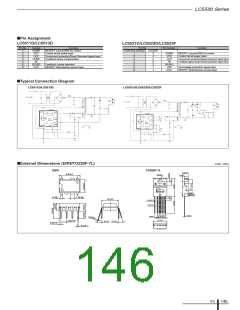
• Two type of packages available: DIP8 (LC551xD/LC552xD) and TO-220F-7L (LC552xF)
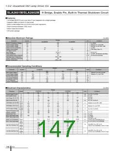
• Built-in startup circuit: eliminates need for external component for startup, reducing the number of components
• Backup possible by using a ceramic capacitor
• Built-in soft start function: reduces load on the power MOSFET and output diodes at power-on
• Built-in leading edge blanking timer: eliminates the need for an external filter, reducing the number of components
• Built-in maximum ON time limiting circuit
• Built-in ON width control circuit
• Protection functions
Overcurrent protection (OCP): Pulse by pulse
Overvoltage protection (OVP): Intermittent oscillation
Overload protection (OLP):
Thermal shutdown (TSD):
Intermittent oscillation
Latch off*
*: Latch off is an operation in which protection is performed while oscillation is stopped.
• Avalanche energy capacity guaranteed by 2-chip structure, simplifying the surge absorption circuit
■Applications
• LED light bulbs
• LED lighting equipment
■Lineup
MOS FET
VDSS(min.)
RDS(ON)
(max.)
3.95Ω
1.9Ω
POUT*
230 VAC/Universal
13W/10W
Part Number
Isolated/Non-isolated
Non-isolated
Package
LC5511D
LC5513D
LC5521D
LC5523D
LC5523F
20W/16W
13W/10W
DIP8
650V
3.95Ω
Isolated
20W/16W
60W/40W
1.9Ω
T0220F-7L
*: The output power values in the table above are those at the rated temperature. Output at 120 to 140% of the rated temperature is possible for the maximum output
power.
Note, however, that the output power may be limited by a low output voltage and by the ON duty specified during transformer design.
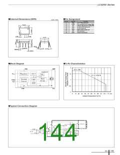
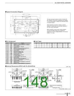
■Electrical Characteristics
Ratings
Parameter
Symbol
Unit
Remarks
min.
typ.
max.
1.Control
Power Supply Startup Operationꢀ
Operation Startup Voltage
Operation Stop Voltage
Circuit Current During Operation
Startup Circuit Operation Voltage
Startup Current
Startup Current Supply Threshold Voltage 1
Startup Current Supply Threshold Voltage 2
Normal Operationꢀ
Vcc(ON)
Vcc(OFF)
Icc(ON)
VSTARTUP
ICC(STARTUP)
Vcc(BIAS)1
Vcc(BIAS)2
13.8
8.4
15.1
9.4
17.3
10.7
3.7
V
V
mA
V
mA
V
V
42
–5.5
9.5
57
72
–3.0
11.0
16.6
–1.0
12.5
18.8
14.4
Minimum Oscillation Frequency
Maximum ON Time
fosc
11.0
30.0
0.55
–10
―
14.0
40.0
0.90
–25
500
0.24
0.17
18.0
50.0
1.25
–40
―
kHz
µs
V
µA
ns
V
TON(max.)
VFB(min.)
IFB(max.)
TBW
VBD(TH1)
VBD(TH2)
FB Pin Control Lower Voltage
Maximum Feedback Current
Leading Edge Blanking Time
Quasi-Resonant Operation Threshold Voltage 1
Quasi-Resonant Operation Threshold Voltage 2
Protection Operationꢀ
0.14
0.12
0.34
0.22
V
Overcurrent Detection Threshold Voltage
OCP Pin Outflow Current
OCP Pin OVP Operation Voltage
OLP Threshold Voltage 1
OLP Threshold Voltage 2
OVP Pin Threshold Voltage
VOCP
IOCP
VBD(OVP)
VFB(OLP)1
VFB(OLP)2
VOVP
–0.54
–120
2.2
5.0
4.1
–0.60
–40
2.6
5.5
4.5
–0.66
–10
3.0
6.0
4.9
V
µA
V
V
V
1.6
2.0
2.4
V
Vcc Pin OVP Operation Voltage
Thermal Shutdown Temperature
Vcc(OVP)
Tj(TSD)
28.5
135
31.5
―
34.0
―
V
℃
2.MOSFET
Drain-Source Voltageꢀ
Drain Leakage Current
VDSS
IDSS
RDS(ON)
RDS(ON)
tf
650
V
µA
300
3.95
1.9
250
400
42
Ω
LC5511D/LC5521D
LC5513D/LC5523D, F
LC5511D/LC5521D
LC5513D/LC5523D, F
Between channel and case for the LC5511D and LC5521D
Between channel and case for the LC5513D and LC5523D
Between channel and internal frame for the LC5523F
ON Resistance
Switching Time
Ω
ns
ns
℃/W
℃/W
℃/W
tf
θch-c
θch-c
θch-F
Thermal Resistance
35.5
3.1
ICs
144

 ETC [ ETC ]