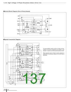
1-2-6 High Voltage 3-Phase Brushless Motor Driver ICs
SCM1100M Series IGBT Output Element, Built-in Shoot Through Prevention and Overcurrent Protection Circuits
■Features
• Each half-bridge circuit consists of a pre-driver circuit that is completely independent from the others
• Protection against simultaneous high- and low-side turning on
• Bootstrap diodes with series resistors for suppressing inrush current are incorporated
• CMOS compatible input (3.3 to 5 V)
• Designed to minimize simultaneous current through both high- and low-side IGBTs by optimizing gate drive resistors
• UVLO protection with auto restart
• Overcurrent protection with off-time period adjustable by an external capacitor
• Fault (FO indicator) signal output at protection activation: UVLO (low side only), OCP, and STP
• Proprietary power DIP package
• UL Recognized Component (File No.: E118037)
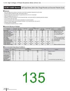
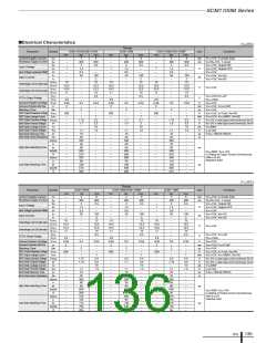
■Absolute Maximum Ratings
(T a=25℃)
a
(T =25℃)
Ratings
Parameter
Symbol
SCM1101M
SCM1103M
SCM1104M
SCM1105MF
SCM1106M
SCM1110MF
Unit
Conditions
(SCM1101MF)
(SCM1104MF)
(SCM1106MF)
Supply Voltage
VBB
VDC(Surge)
VCES
VCC
450
500
600
20
20
450
500
600
20
20
5
10
450
500
600
20
20
450
500
600
20
20
15
30
–0.5 to +7
7
41.6
450
500
600
20
20
450
500
600
20
20
15
30
–0.5 to +7
7
41.6
V
V
V
V
V
A
A
V
V
W
Between VBB and LS1 to LS3
Between VBB and LS1 to LS3
VCC=15V,IC=1mA,VIN=0V
VCC1 to 3 and COM1 to COM3
VB1 to VB3 and HS (U,V,W)
Supply Voltage (Surge)
IGBT Output Withstand Voltage
Control Supply Voltage
Control Supply Voltage (Bootstrap)
Output Current (continuous)
Output Current (pulse)
Input Voltage
VBS
Io
Iop
10
20
8
16
10
20
T≤1ms
VIN
–0.5 to +7
7
–0.5 to +7
7
19.8
6.3
6.5
–20 to +100
150
–40 to +150
2000
–0.5 to +7
7
–0.5 to +7
7
HIN1 to HIN3 or LIN1 to LIN3 and COM1 to COM3
FO Pin Voltage
Power Dissipation
VFO
FO1 to FO3 and COM1 to COM3
PD
20.8(33.7)
6(3.7)
6.5(4.2)
–20 to +100
150
20.1(32.8)
6.2(3.8)
6.5(4.2)
–20 to +100
150
20.8(33.7)
6(3.7)
6.5(4.2)
–20 to +100
150
Tc=25°C while one IGBT element operates
Thermal Resistance (IGBT)
Thermal Resistance (FRD)
Operating Case Temperature
Junction Temperature
Storage Temperature
R(j-c)Q
R(j-c)F
TOP
3
4
3
4
°C/W Per IGBT element
°C/W Per FRD element
°C
°C
°C
–20 to +100
150
–40 to +150
2000
–20 to +100
150
–40 to +150
2000
Tj
Tstg
Viso
–40 to +150
2000
–40 to +150
2000
–40 to +150
2000
Insulation Withstand Voltage
V
Between rear and lead pins, AC one minute
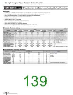
■Recommended Operating Conditions
Ratings
Parameter
Symbol
SCM1100M Series
Unit
Conditions
min.
–
typ.
300
–
–
–
–
–
–
–
max.
400
16.5
–
–
–
22
10
5.5
220
20
Main Supply Voltage
VDC
VCC,VBS
tINmin(on)
tINmin(off)
tdead
V
V
Between VBB and LS
Control Supply Voltage
13.5
0.5
0.5
1.0
1
µs
µs
µs
kΩ
nF
V
uF
kHz
°C
ON pulse
OFF pulse
Minimum Input Pulse Width
Input Signal Dead Time
FO Pull-up Resistor
CFO Capacitor Capacity
FO Pull-up Voltage
RFO
CFO
1
VFO
4.5
10
–
Boot Capacitor
CBOOT
fc
–
–
–
PWM Carrier Frequency
Junction Temperature
For the SCM1101M (F) and SCM1105MF: 10
Tj
–
125
ICs
134

 ETC [ ETC ]