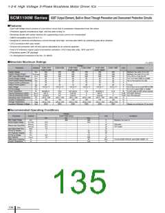
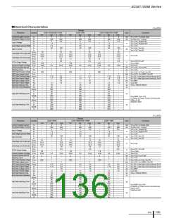
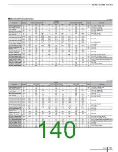
SCM1100M Series
■Electrical Characteristics
(Ta=25℃)
Ratings
Parameter
Symbol
SCM1101M/SCM1101MF
SCM1103M
SCM1104M/SCM1104MF
Unit
Conditions
min.
–
–
–
1
–
–
–
typ.
5
400
2
1.5
0.5
50
–
max.
8
800
2.5
–
–
100
2
min.
–
–
–
1
–
–
–
typ.
5
400
2
1.5
0.5
50
–
max.
8
800
2.5
–
–
100
2
min.
–
–
–
1
–
–
–
typ.
5
400
2
1.5
0.5
50
–
max.
Control Supply Current
Bootstrap Supply Current
ICC
Ibs
8
800
2.5
–
–
100
2
mA
uA
VCC=15V, 3 circuits total
VB-HS=15V, 1 circuit
VCC=15V, Output:ON
VCC=15V, Output:OFF
VCC=15V
VIH
Input Voltage
VIL
V
Input Voltage Hysteresis Width
Input Current
VH
IIH
VCC=15V, VIN=5V
VCC=15V, VIN=0V
µA
IIL
VUVHL
VUVHH
VUVLL
VUVLH
VFOL
VFOH
VTRIP
tP
10
10.5
10.5
11
–
4.8
0.46
2
–
600
–
–
–
–
–
–
–
–
–
–
–
–
–
–
–
–
–
0.5
–
2
–
–
1.75
1.7
–
1.1
70
22
320
50
80
560
210
350
80
140
610
200
12
12.5
12.5
13
0.5
–
0.54
–
–
10
10.5
10.5
11
–
4.8
0.46
2
–
600
–
–
–
–
–
–
–
–
–
–
–
–
–
–
–
–
–
0.5
–
2
–
–
1.7
1.4
–
1.1
70
22
340
60
80
430
240
380
90
100
500
220
12
12.5
12.5
13
0.5
–
0.54
–
–
10
10.5
10.5
11
–
4.8
0.46
2
–
600
–
–
–
–
–
–
–
–
–
–
–
–
–
–
–
–
–
0.5
–
2
–
–
1.75
1.6
–
1.1
70
22
360
70
80
560
210
420
110
140
630
210
12
12.5
12.5
13
0.5
–
0.54
–
–
Undervoltage Lock Out (high side)
Undervoltage Lock Out (low side)
FO Pin Output Voltage
V
VCC=15V
VCC=15V,VFO=5V
RFO=10kΩ
VCC=15V
V
Overcurrent Protection Trip Voltage
Overcurrent Protection Hold Time
Blanking Time
V
ms
µs
V
mA
V
V
µA
V
VCC=15V, CFO=2.2nF
VCC=15V
tbk
IGBT Output Breakdown Voltage
IGBT Output Leakage Current
IGBT Output Saturation Voltage
Boot Diode Forward Voltage
Boot Diode Leakage Current
Boot Diode Forward Voltage
Boot Diode Recovery Time
Boot Diode Series Resistance
VCES
ICES
–
1
–
1
–
1
VCC=15V, IC=1mA, VIN=0V
VCC=15V, VCE=600V, VIN=0V
VCE(sat)
2.2
2.2
10
1.3
–
–
–
–
–
–
–
–
–
–
–
–
2.1
2
10
1.3
–
–
–
–
–
–
–
–
–
–
–
–
2.2
2.2
10
1.3
–
–
–
–
–
–
–
–
–
–
–
–
V
CC=15V, I =rated output current (continuous) VIN=5V
C
VF
VCC=15V, IF=rated output current (continuous), VIN=0V
IIB
VR=600V
IF=0.15A
IF/IRP=100mA/100mA
VFB
trr
ns
Ω
RB
td(on)
tr
trr
td(off)
tf
td(on)
tr
trr
td(off)
tf
High Side Switching Time
Low Side Switching Time
ns
V
DC=300V, VCC=15V
–
–
–
–
–
–
–
–
–
–
–
–
–
–
–
–
–
–
I
C=Rating of Output Current (Continuous)
HIN=0 to 5V
Inductive load
ns
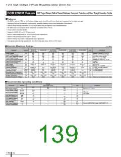
(Ta=25℃)
Ratings
Parameter
Symbol
SCM1105MF
SCM1106M/SCM1106MF
SCM1110MF
Unit
Conditions
min.
–
–
–
1
–
–
–
typ.
5
400
2
1.5
0.5
50
–
max.
8
800
2.5
–
–
100
2
min.
–
–
–
1
–
–
–
typ.
5
400
2
1.5
0.5
50
–
max.
min.
–
–
–
1
–
–
–
typ.
5
400
2
1.5
0.5
50
–
max.
8
800
2.5
–
–
100
2
Control Supply Current
Bootstrap Supply Current
ICC
Ibs
8
800
2.5
–
–
100
2
mA
uA
VCC=15V, 3 circuits total
VB-HS=15V, 1 circuit
VCC=15V, Output:ON
VCC=15V, Output:OFF
VCC=15V
VIH
Input Voltage
VIL
V
Input Voltage Hysteresis Width
Input Current
VH
IIH
VCC=15V, VIN=5V
VCC=15V, VIN=0V
µA
IIL
VUVHL
VUVHH
VUVLL
VUVLH
VFOL
VFOH
VTRIP
tP
10
10.5
10.5
11
–
4.8
0.46
2
–
600
–
–
–
–
–
–
–
–
–
–
–
–
–
–
–
–
–
0.5
–
2
–
–
1.75
1.75
–
1.1
70
22
365
80
90
690
200
415
135
115
790
205
12
12.5
12.5
13
0.5
–
0.54
–
–
10
10.5
10.5
11
–
4.8
0.46
2
–
600
–
–
–
–
–
–
–
–
–
–
–
–
–
–
–
–
–
0.5
–
2
–
–
2.2
1.7
–
1.1
70
22
320
50
80
490
80
350
80
140
540
80
12
12.5
12.5
13
0.5
–
0.54
–
–
10
10.5
10.5
11
–
4.8
0.46
2
–
600
–
–
–
–
–
–
–
–
–
–
–
–
–
–
–
–
–
0.5
–
2
–
–
2.2
1.75
–
1.1
70
22
365
80
90
650
85
415
135
115
755
85
12
12.5
12.5
13
0.5
–
0.54
–
–
Undervoltage Lock Out (high side)
Undervoltage Lock Out (low side)
FO Pin Output Voltage
V
VCC=15V
VCC=15V, VFO=5V
RFO=10kΩ
VCC=15V
V
Overcurrent Protection Trip Voltage
Overcurrent Protection Hold Time
Blanking Time
V
ms
µs
V
mA
V
V
µA
V
VCC=15V,CFO=2.2nF
VCC=15V
tbk
IGBT Output Breakdown Voltage
IGBT Output Leakage Current
IGBT Output Saturation Voltage
Boot Diode Forward Voltage
Boot Diode Leakage Current
Boot Diode Forward Voltage
Boot Diode Recovery Time
Boot Diode Series Resistance
VCES
ICES
–
1
–
1
–
1
VCC=15V, IC=1mA, VIN=0V
VCC=15V, VCE=600V, VIN=0V
V
CE(sat)
2.2
2.2
10
1.3
–
–
–
–
–
–
–
–
–
–
–
–
2.6
2.2
10
1.3
–
–
–
–
–
–
–
–
–
–
–
–
2.6
2.2
10
1.3
–
–
–
–
–
–
–
–
–
–
–
–
V
CC=15V, I =rated output current (continuous) VIN=5V
C
VF
VCC=15V, IF=rated output current (continuous), VIN=0V
IIB
VR=600V
IF=0.15A
IF/IRP=100mA/100mA
VFB
trr
ns
Ω
RB
td(on)
tr
trr
td(off)
tf
td(on)
tr
trr
td(off)
tf
High Side Switching Time
Low Side Switching Time
ns
V
DC=300V, VCC=15V
–
–
–
–
–
–
–
–
–
–
–
–
–
–
–
–
–
–
IC=Rating of Output Current (Continuous)
HIN=0 to 5V
Inductive load
ns
ICs
135

 ETC [ ETC ]