1-2-6 High Voltage 3-Phase Brushless Motor Driver ICs
SLA6805MP IGBT Output Element, Built-in Overcurrent Protection Circuit
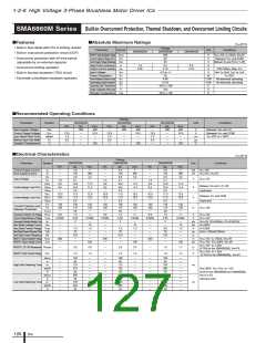
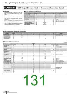
■Features
■Absolute Maximum Ratings
(Ta=25°C)
• A package including 6 units each of IGBT and
FRD for 3-phase bridge, and pre-drive (HVIC,
LVIC)
Parameter
Symbol
Ratings
Unit
V
Conditions
Vcc=15V, VIN=0V
Between VCC and COM
Between V and HS (U, V, W)
IGBT Output Voltage
VCES
600
Control Supply Voltage
Control Supply Voltage (bootstrap)
Output Current (continuous)
Output Current (pulse)
Input Voltage
Vcc
20
V
• Best for driving a refrigerator compressors and
dishwashing driers
V
BS
20
V
B
Io
Iop
3
6
A
A
PW≤100µs, duty=1%
Tc=25°C
• High side drive of bootstrap method has been
employed.
V
IN
–0.5 to +7
32.8
V
Power Dissipation
P
D
W
• Built-in undervoltage lock out (auto regression)
• Built-in overcurrent protection circuit
3.8
°C/W
°C/W
°C
°C
°C
When all IGBT elements operating
When all FRD elements operating
Thermal Resistance (Junction to Case)
θ
j–c
5.4
Operating Case Temperature
Junction Temperature (Power part)
Storage Temperature
Top
Tch
Tstg
–20 to +100
+150
• Built-in fail signal output function (for when the
overcurrent protection circuit activates)
–40 to +150
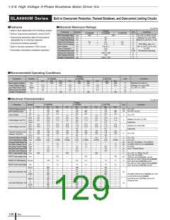
■Recommended Operating Conditions
Ratings
Parameter
Symbol
Unit
Conditions
min.
–
typ.
300
–
max.
450
16.5
–
Main Supply Voltage
Control Supply Voltage
Input Signal Dead Time
Minimum Input Pulse Width
Junction Temperature
VBB
Vcc
tdead
tw
V
V
Between VBB and LS
13.5
1.5
0.5
–
Between VCC and COM
–
µs
µs
°C
–
–
Tj
–
125
■Electrical Characteristics
(Ta=25°C)
Ratings
typ.
4
Parameter
Control Supply Current
Input Voltage
Symbol
Unit
mA
V
Conditions
min.
–
max.
6
Icc
Vcc=15V
V
IH
IL
Ihys
IH
IL
UVHL
–
2
2.5
–
Vcc=15V, Output:ON
Vcc=15V, Output:OFF
Vcc=15V
V
1
1.5
0.5
50
Input Voltage Hysteresis Width
Input Current
V
–
–
V
I
–
100
2
Vcc=15V, VIN=5V
Vcc=15V, VIN=0V
µA
I
–
–
V
9.0
9.5
–
10.0
10.5
0.5
11.0
11.5
0.5
–
11.0
11.5
–
Undervoltage Lock Out
(High Side)
V
UVHH
V
Between VB and U (V, W)
V
UVhys
V
UVLL
UVLH
UVhys
10.0
10.5
–
12.0
12.5
–
Undervoltage Lock Out
(Low Side)
V
V
V
Between VCC and COM
Vcc=15V
V
V
FOL
0
1.0
5.5
0.55
–
FO Pin Output Voltage
V
FOH
4.0
0.45
–
–
Overcurrent Protection Trip Voltage
Blanking Time
V
TRIP
0.5
2
V
us
V
Vcc=15V
Vcc=15V
tbk
IGBT Output Breakdown Voltage
IGBT Output Leakage Current
IGBT Output Saturation Voltage
Diode Forward Voltage
V
CES
600
–
–
–
Vcc=15V, Ic=1
mA, VIN=0V
ICES
–
1
mA
Vcc=15V, VCES=600V, VIN=0V
V
CE(sat)
–
1.75
1.65
365
55
2.1
2
V
V
Vcc=15V, VIN=5V, I
C
=3A
V
EC
–
Vcc=15V, VIN=0V, IF
=3A
td(on)
tr
–
–
–
–
High Side Switching Time
Low Side Switching Time
trr
–
80
–
ns
ns
td(off)
tf
–
365
170
395
60
–
V
BB=300V, Vcc=15V,
–
–
Ic=3A, VIN=0 to 5V,
inductive load
td(on)
tr
–
–
–
–
trr
–
75
–
td(off)
tf
–
395
170
–
–
–
ICs
130

 ETC [ ETC ]